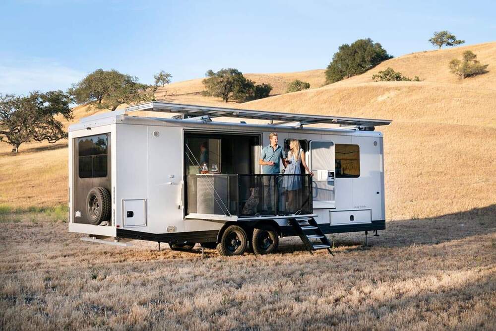
Sorry I’m not that active. My mom had a heart attack a little over a month ago and I care for her now. Plus last Thursday I went to the ER for overdosing accidentally on depakote which can be deadly. But check this out. In case of an emergency is this cool or what? Kind of expensive though.
If this summer you’re in the mood for some off-the-grid camping trips, this state-of-the-art self-sustainable luxury trailer is what you need. Designed from the ground up for off-grid camping, the trailer can also produce its own water, making it fully self-sufficient. This extremely sophisticated camper is the work of a California-based company called Living Vehicle which specializes in making self-sustainable luxury travel trailers. The 2023 model was recently introduced by Living Vehicle and it boasts a few industry firsts.
According to its makers, the off-grid camper is aimed at those who wish “to travel far away from campgrounds and overcrowded RV parks.” With a starting price of $340,000, the luxury camper is available in three versions: Core, Max, and Pro. Additionally, Living Vehicle offers a laundry list of options that can be added to the camper via the company’s online configurator.
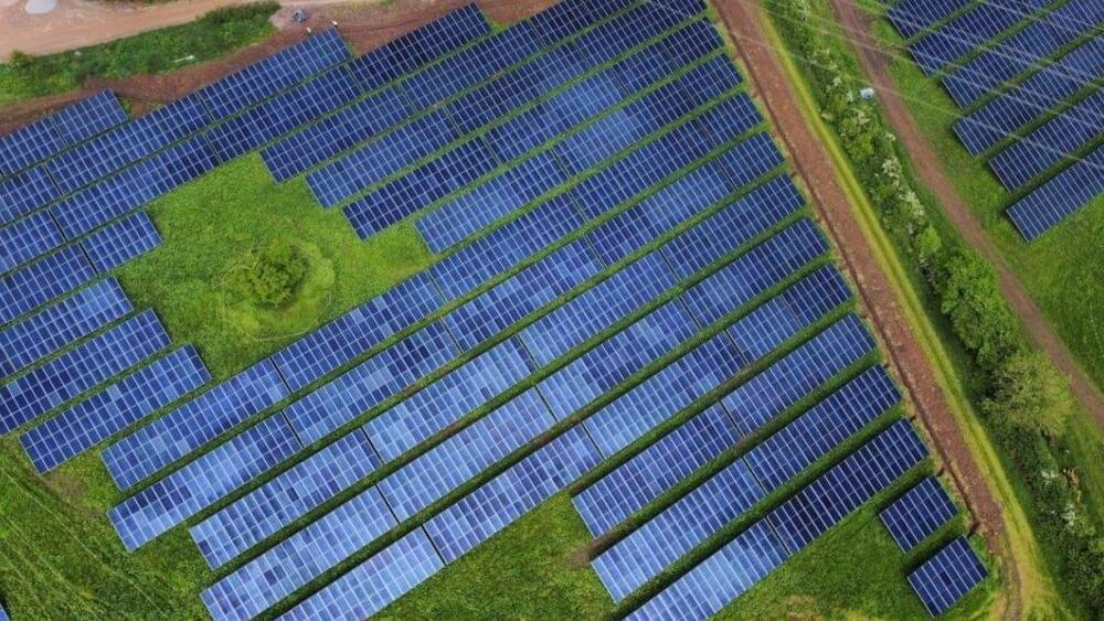
The 29-foot-long innovative camper runs on solar power. It comes with 1,400W of solar capacity as standard, but Living Vehicle offers an option to further increase its capacity. The Pro version boosts the maximum solar capacity of 3,400W. The energy is stored in a lithium-ion battery pack with a capacity ranging from 14.4 kWh to 57.6 kWh depending on the trailer’s version, along with invertor power ranging from 5 kW to 20 kW. The company from Santa Barbara claims the stored solar energy can power the camper’s air conditioner overnight without any external power input.


