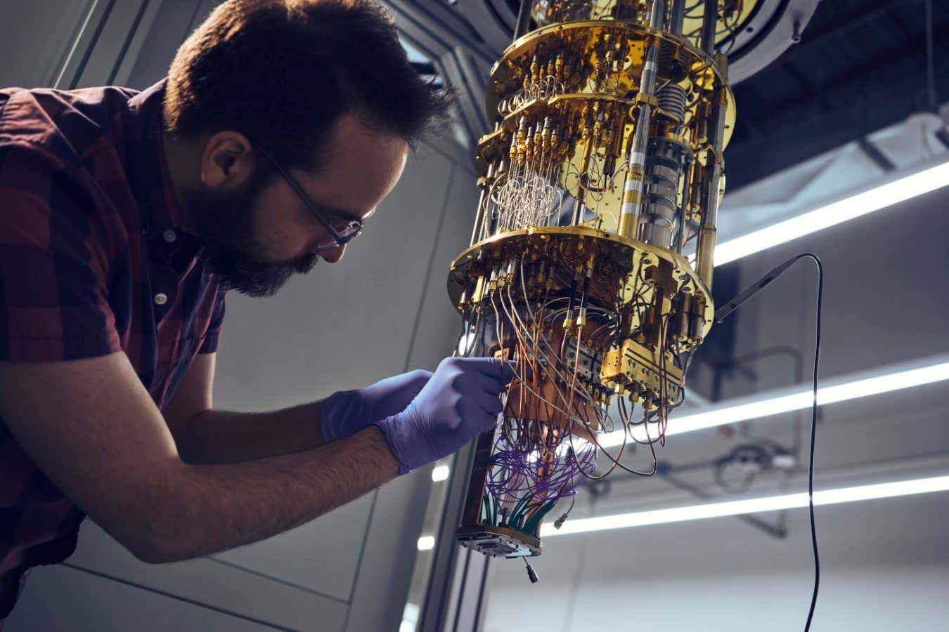
Researchers demonstrated a novel entangling quantum logic gate that operates on four-level photonic systems (qudits).
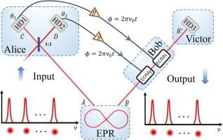
As an important quantum communication protocol, quantum teleportation has broad applications in quantum information science and technology. For the application, it is essential to enhance the ability of quantum teleportation by teleporting multiple quantum states simultaneously. Here, we experimentally demonstrate deterministic quantum teleportation of multiple sideband qumodes of coherent states, which corresponds to teleporting multiple quantum states simultaneously, with the assistance of continuous-variable (CV) quantum entanglement. By fine-tuning the phases of two classical channels according to different adjustable frequencies, we successfully realize deterministic CV quantum teleportation with up to 5 sideband qumodes simultaneously within the frequency bandwidth of 24 MHz.
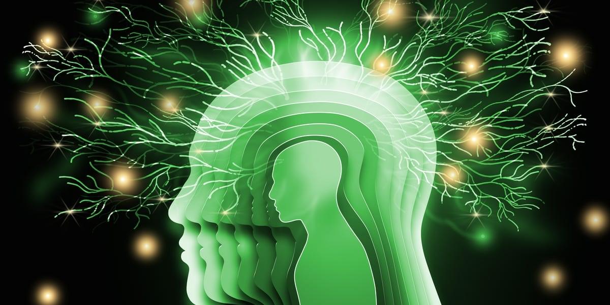
But what if our biological makeup limits how creative we can be? Maybe the timing of the clock that governs our introspections forces our intuitive periods—or the times of uncertainty—to be too brief. Could we use our quantum technologies to extend the wavelike processing inside our brains? I am here inspired by Aldous Huxley, who suggested in his famous book, The Doors of Perception, that drugs could alter our consciousness, revealing true reality. But rather than using drugs, I envision quantum chips designed to suppress the “noise” that induces introspection, allowing a longer interference period for our intuitive thoughts to develop. This has the potential to be far more potent than what Huxley could ever have imagined.
For my idea to work, we would first have to understand where and how these superpositions are stored and manipulated in the brain. The British physicist Roger Penrose, PhD, has speculated that this occurs within microtubules, which are dynamic, hollow, rod-like components of the eukaryotic cytoskeleton that are responsible for things such as intercellular transport. Despite some circumstantial evidence, we do not have a strong reason to believe that microtubules are capable of quantum interference, but they are certainly worth further investigation. Once we understand how our brain uses quantum effects, we could then design a quantum chip that interfaces with the relevant biological components. Theoretically, the device would be able to upload superposition states to store them for longer periods and shield them from collapse, helping us to enhance our creative wavelike thinking.
One wonders what kind of power would be unleashed by doing this. I imagine the change would not be purely quantitative, so that we merely become faster calculators or quicker problem solvers, although even that would be amazing. Instead, I think the change could be qualitative, expanding our perception into a completely different realm, effectively creating a new species. We might theoretically become more powerful than modern humans, just as we currently are with respect to other apes. Quantum-enhanced humans would see further domains of reality that would otherwise remain hidden forever from us ordinary humans.

Preserving quantum information is key to developing useful quantum computing systems. But interacting quantum systems are chaotic and follow laws of thermodynamics, eventually leading to information loss. Physicists have long known of a strange exception, called dynamical freezing, when quantum systems shaken at precisely tuned frequencies evade these laws. But how long can this phenomenon postpone thermodynamics?
Not forever, but for an astonishingly long time, Cornell physicists have determined, giving the first quantitative answer. Using a new mathematical framework, they demonstrate that the frozen state can be stabilized long enough to be a useful strategy for preserving information in quantum systems. This can be a promising route for maintaining coherence in quantum computers as the numbers of qubits scale up to the millions.
“It’s like asking, how do you evade the laws of physics from eventually taking over?” said Debanjan Chowdhury, associate professor of physics in the College of Arts and Sciences. “Imagine that you had a hot cup of coffee that even without a heater, stayed hot. Or a block of ice placed on a heater that never melts. Is that even possible? This has been one of the big open problems in the field of quantum many-body systems.”
Superconducting computing circuits were briefly heralded as the future of computing in the 1980s. Columnist Karmela Padavic-Callaghan visits a quantum chip foundry where one company is betting this technology’s second act will revolutionise quantum computers.
Identifying the boundary between classical and quantum computation is a central challenge in quantum information. In multi-qubit systems, entanglement and magic are the key resources underlying genuinely quantum behaviour. While entanglement is well understood, magic — essential for universal quantum computation — remains relatively poorly characterised. Here we show that determining membership in the stabilizer polytope, which defines the free states of magic-state resource theory, requires super-exponential time $\exp( n^2)$ in the number of qubits $n$, even approximately. We reduce the problem to solving a $3$-SAT instance on $n^2$ variables and, by invoking the exponential time hypothesis, the result follows. As a consequence, both quantifying and certifying magic are fundamentally intractable: any magic monotone for general states must be super-exponentially hard to compute, and deciding whether an operator is a valid magic witness is equally difficult. As a corollary, we establish the robustness of magic as computationally optimal among monotones. This barrier extends even to classically simulable regimes: deciding whether a state lies in the convex hull of states generated by a logarithmic number of non-Clifford gates is also super-exponentially hard. Together, these results reveal intrinsic computational limits on assessing classical simulability, distilling pathological magic states, and ultimately probing and exploiting magic as a quantum resource.
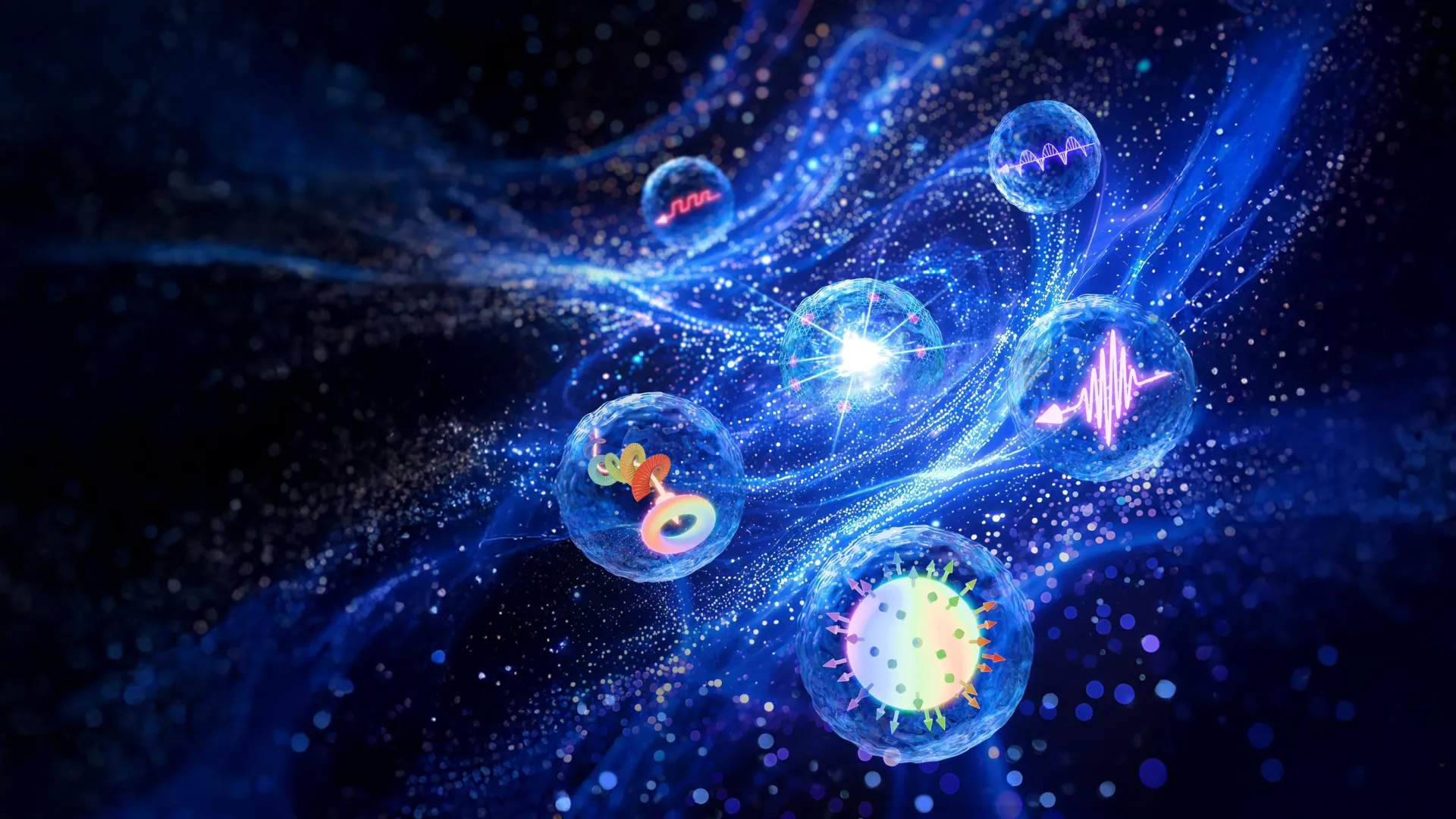
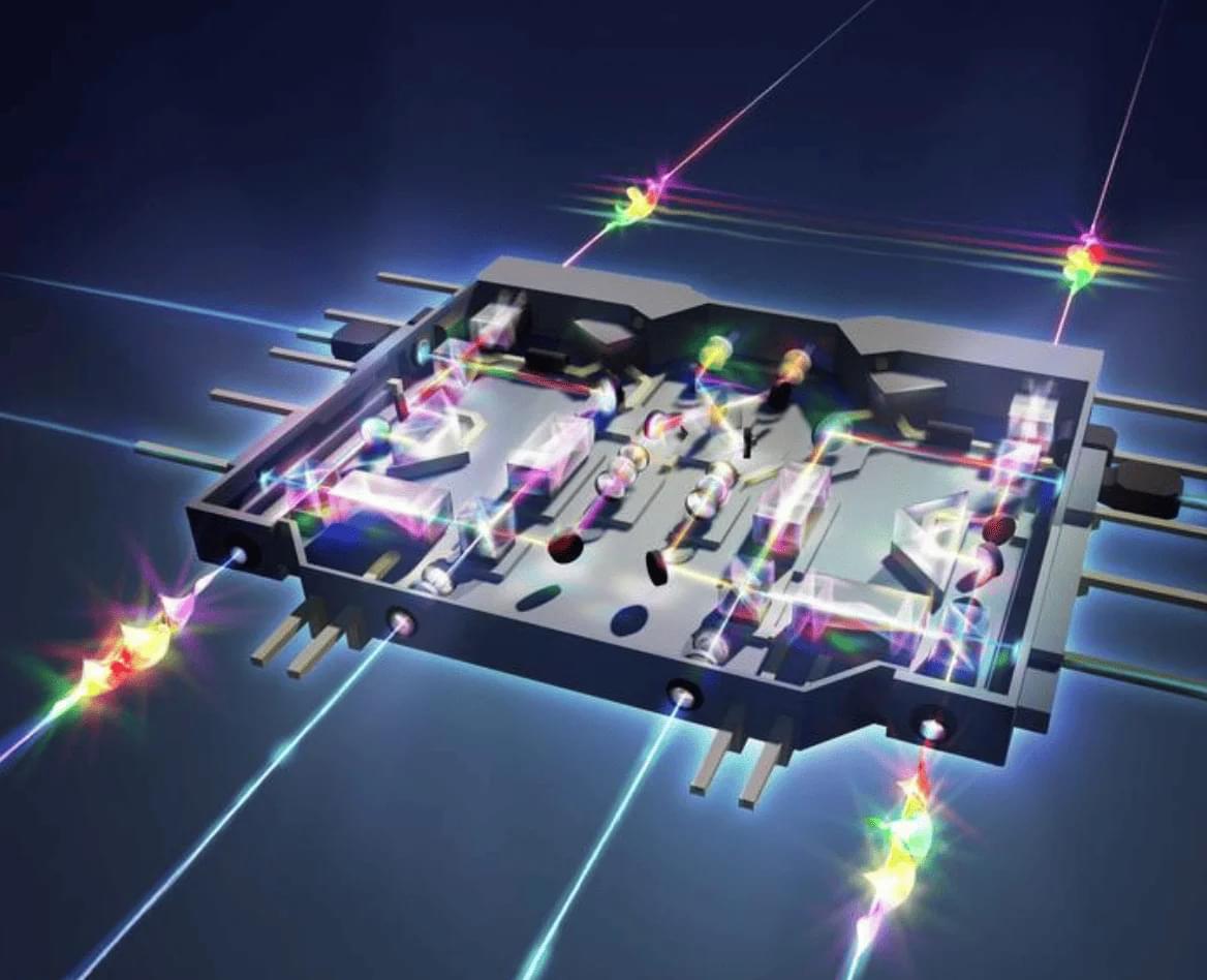
Researchers have discovered new ways to shape quantum light, creating high-dimensional states that can carry much more information per photon. Using advanced tools like on-chip photonics and ultrafast light structuring, they’re pushing quantum communication and imaging into exciting new territory. Although long-distance transmission remains tricky, innovative approaches—such as topological quantum states—could make these fragile signals far more resilient. The momentum suggests quantum optics is entering a bold new phase.
Workshop on quantum aspects of black holes and spacetime.
Topic: Comments on the Hartle-Hawking state and observers.
Speaker: Ying Zhao.
Affiliation: Massachusetts Institute of Technology.
Date: December 3, 2025
Wolfensohn Hall.
It was argued that any fixed holographic theory contains only one closed universe state and hence fails to give semi-classical physics. It was proposed that this problem can be resolved by including a classical observer living inside the universe. Earlier works focused on closed universes connected with asymptotic Euclidean boundaries. In this talk we examine the case of Hartle-Hawking state where the dominant Euclidean topology is a sphere. We show that different features emerge. We comment on the potential implications for the understanding of de Sitter space. Based on work with Daniel Harlow.