Quantum-enhanced single-parameter estimation is an established capability, with non-classical probe states achieving precisions beyond what can be reached by the equivalent classical resources in photonic1,2,3, trapped-ion4,5, superconducting6 and atomic7,8 systems. This has paved the way for quantum enhancements in practical sensing applications, from gravitational wave detection9 to biological imaging10. For single-parameter estimation, entangled probe states are sufficient to reach the ultimate allowed precisions. However, for multi-parameter estimation, owing to the possible incompatibility of different observables, entangling resources are also required at the measurement stage. The ultimate attainable limits in quantum multi-parameter estimation are set by the Holevo Cramér–Rao bound (Holevo bound)11,12. In most practical scenarios, it is not feasible to reach the Holevo bound as this requires a collective measurement on infinitely many copies of the quantum state13,14,15,16 (see Methods for a rigorous definition of collective measurements). Nevertheless, it is important to develop techniques that will enable the Holevo bound to be approached, given that multi-parameter estimation is fundamentally connected to the uncertainty principle17 and has many physically motivated applications, including simultaneously estimating phase and phase diffusion18,19, quantum super-resolution20,21, estimating the components of a three-dimensional field22,23 and tracking chemical processes24. Furthermore, as we demonstrate, collective measurements offer an avenue to quantum-enhanced sensing even in the presence of large amounts of decoherence, unlike the use of entangled probe states25,26.
To date, collective measurements for quantum multi-parameter metrology have been demonstrated exclusively on optical systems27,28,29,30,31,32. Contemporary approaches to collective measurements on optical systems are limited in their scalability: that is, it is difficult to generalize present approaches to measuring many copies of a quantum state simultaneously. The limited gate set available can also make it harder to implement an arbitrary optimal measurement. Indeed, the collective measurements demonstrated so far have all been restricted to measuring two copies of the quantum state and, while quantum enhancement has been observed, have all failed to reach the ultimate theoretical limits on separable measurements33,34. Thus, there is a pressing need for a more versatile and scalable approach to implementing collective measurements.
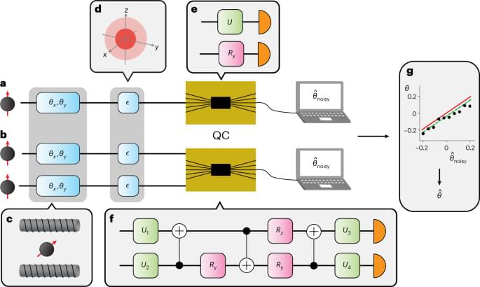
In this work, we design and implement theoretically optimal collective measurement circuits on superconducting and trapped-ion platforms. The ease with which these devices can be reprogrammed, the universal gate set available and the number of modes across which entanglement can be generated, ensure that they avoid many of the issues that current optical systems suffer from. Using recently developed error mitigation techniques35 we estimate qubit rotations about the axes of the Bloch sphere with a greater precision than what is allowed by separable measurements on individual qubits. This approach allows us to investigate several interesting physical phenomena: we demonstrate both optimal single-and two-copy collective measurements reaching the theoretical limits33,34. We also implement a three-copy collective measurement as a first step towards surpassing two-copy measurements. However, due to the circuit complexity, this measurement performs worse than single-copy measurements. We investigate the connection between collective measurements and the uncertainty principle. Using two-copy collective measurements, we experimentally violate a metrological bound based on known, but restrictive uncertainty relations36. Finally, we compare the metrological performance of quantum processors from different platforms, providing an indication of how future quantum metrology networks may look.


