Quantum computers, devices that perform computations by exploiting quantum mechanical phenomena, have the potential to outperform classical computers on some tasks and optimization problems. In recent years, research teams at both academic institutions and IT companies have been trying to realize this predicted better performance for specific problems, which is broadly known as “quantum advantage.”
To reliably demonstrate that a quantum computer performs better than a classical computer, one should, among other things, collect precise measurements inside the computer and compare them to those collected in classical computers. Doing this, however, can sometimes be challenging, due to the distinct nature of these two types of devices.
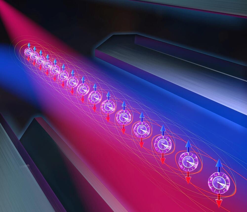
Researchers at NIST/University of Maryland, UC Berkeley, Caltech and other institutes in the United States recently introduced and tested a new protocol that could help to reliably validate the advantage of quantum computers. This protocol, introduced in Nature Physics, relies on mid-circuit measurements and a cryptographic technique.


 עברית (Hebrew)