Menu

Blog

Archive for the ‘quantum physics’ category: Page 417

May 13, 2021

New evidence for electron’s dual nature found in a quantum spin liquid

Posted by in categories: particle physics, quantum physics

A new discovery led by Princeton University could upend our understanding of how electrons behave under extreme conditions in quantum materials. The finding provides experimental evidence that this familiar building block of matter behaves as if it is made of two particles: one particle that gives the electron its negative charge and another that supplies its magnet-like property, known as spin.

“We think this is the first hard evidence of spin-charge separation,” said Nai Phuan Ong, Princeton’s Eugene Higgins Professor of Physics and senior author on the paper published this week in the journal Nature Physics.

The fulfill a prediction made decades ago to explain one of the most mind-bending states of matter, the quantum spin liquid. In all materials, the spin of an electron can point either up or down. In the familiar magnet, all of the spins uniformly point in one direction throughout the sample when the below a .

May 12, 2021

New atomically precise graphene nanoribbon heterojunction sensor developed

Posted by in categories: particle physics, quantum physics

An international research team led by the University of Cologne has succeeded for the first time in connecting several atomically precise nanoribbons made of graphene, a modification of carbon, to form complex structures. The scientists have synthesized and spectroscopically characterized nanoribbon heterojunctions. They then were able to integrate the heterojunctions into an electronic component. In this way, they have created a novel sensor that is highly sensitive to atoms and molecules. The results of their research have been published under the title Tunneling current modulation in atomically precise graphene nanoribbon heterojunctions’ in Nature Communications. The work was carried out in close cooperation between the Institute for Experimental Physics with the Department of Chemistry at the University of Cologne, as well as with research groups from Montreal, Novosibirsk, Hiroshima, and Berkeley. It was funded by the German Research Foundation (DFG) and the European Research Council (ERC).

The heterojunctions of graphene nanoribbons are just one nanometer—one millionth of a millimeter—wide. Graphene consists of only a single layer of carbon atoms and is considered the thinnest material in the world. In 2010, researchers in Manchester succeeded in making single-atom layers of graphene for the first time, for which they won the Nobel Prize. The heterojunctions used to make the sensor are each seven and fourteen carbon atoms wide and about 50 nanometres long. What makes them special is that their edges are free of defects. This is why they are called atomically precise nanoribbons, explained Dr. Boris Senkovskiy from the Institute for Experimental Physics. The researchers connected several of these nanoribbon heterojunctions at their short ends, thus creating more complex heterostructures that act as tunneling barriers.

The heterostructures were investigated using angle-resolved photoemission, optical spectroscopy, and scanning tunneling microscopy. In the next step, the generated heterostructures were integrated into an electronic device. The flowing through the nanoribbon heterostructure is governed by the quantum mechanical tunneling effect. This means that under certain conditions, electrons can overcome existing energy barriers in atoms by ‘tunneling,’ so that a current then flows even though the barrier is greater than the available energy of the electron.

May 12, 2021

Intel says it has solved a key bottleneck in quantum computing

Posted by in categories: computing, quantum physics

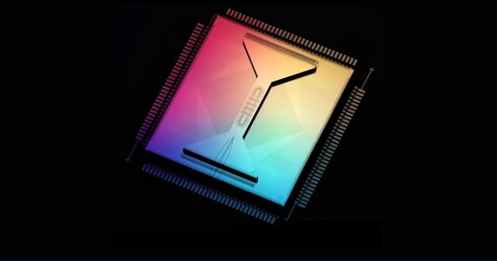
Intel has overcome a quantum computing bottleneck by controlling two qubits with a cryogenic control chip.

May 12, 2021

CES 2021: Quantum Operation shows a prototype of a Wearable with Noninvasive glucose monitoring feature

Posted by in categories: biotech/medical, quantum physics, wearables

CES 2021 is blowing up with a lot of announcements despite being a virtual event. Among the lot, a Japanese Startup now says that its wearable can help you monitor Blood Glucose without piercing your skin.

Quantum Operation Inc., has showcased a prototype of a Wearable that typically is like a Smartwatch. It says that the wearable can measure and monitor the Glucose levels in Blood precisely in addition to heart rate and ECG. Apparently, this is possible due to the presence of a Spectrometer inside.

May 12, 2021

Physicists unveil the condensation of liquid light in a semiconductor one-atom-thick

Posted by in categories: computing, particle physics, quantum physics

An international team of physicists has shown experimentally for the first time how a Bose-Einstein condensate — tens of thousands of quanta of ‘liquid light’ — is formed in the thinnest monatomic film of a semiconductor crystal. The team includes the head of the Spin Optics Laboratory at St Petersburg University, Professor Alexey Kavokin. This discovery will help create new types of lasers capable of producing qubits — the main integral parts of quantum computers of the future.

May 10, 2021

Nanotechnology Breakthrough: A Material-Keyboard Made of Graphene

Posted by in categories: nanotechnology, quantum physics

Researchers at ETH Zurich have succeeded in turning specially prepared graphene flakes either into insulators or into superconductors by applying an electric voltage. This technique even works locally, meaning that in the same graphene flake regions with completely different physical properties can be realized side by side.

The production of modern electronic components requires materials with very diverse properties. There are isolators, for instance, which do not conduct electric current, and superconductors which transport it without any losses. To obtain a particular functionality of a component one usually has to join several such materials together. Often that is not easy, in particular when dealing with nanostructures that are in widespread use today.

A team of researchers at ETH Zurich led by Klaus Ensslin and Thomas Ihn at the Laboratory for Solid State Physics have now succeeded in making a material behave alternately as an insulator or as a superconductor – or even as both at different locations in the same material – by simply applying an electric voltage. Their results have been published in the scientific journal Nature Nanotechnology. The work was supported by the National Centre of Competence in Research QSIT (Quantum Science and Technology).

May 10, 2021

Complex shapes of photons to boost future quantum technologies

Posted by in categories: computing, neuroscience, quantum physics

As the digital revolution has now become mainstream, quantum computing and quantum communication are rising in the consciousness of the field. The enhanced measurement technologies enabled by quantum phenomena, and the possibility of scientific progress using new methods, are of particular interest to researchers around the world.

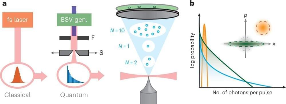
Recently two researchers at Tampere University, Assistant Professor Robert Fickler and Doctoral Researcher Markus Hiekkamäki, demonstrated that two– interference can be controlled in a near-perfect way using the spatial shape of the photon. Their findings were recently published in the prestigious journal Physical Review Letters.

“Our report shows how a complex light-shaping method can be used to make two quanta of light interfere with each other in a novel and easily tuneable way,” explains Markus Hiekkamäki.

May 10, 2021

Physicists observe modified energy landscapes at the intersection of 2D materials

Posted by in categories: computing, particle physics, quantum physics

In 1884, Edwin Abbott wrote the novel Flatland: A Romance in Many Dimensions as a satire of Victorian hierarchy. He imagined a world that existed only in two dimensions, where the beings are 2D geometric figures. The physics of such a world is somewhat akin to that of modern 2D materials, such as graphene and transition metal dichalcogenides, which include tungsten disulfide (WS2), tungsten diselenide (WSe2), molybdenum disulfide (MoS2) and molybdenum diselenide (MoSe2).

Modern 2D materials consist of single-atom layers, where electrons can move in two dimensions but their motion in the third dimension is restricted. Due to this ‘squeeze’, 2D materials have enhanced optical and that show great promise as next-generation, ultrathin devices in the fields of energy, communications, imaging and quantum computing, among others.

Typically, for all these applications, the 2D materials are envisioned in flat-lying arrangements. Unfortunately, however, the strength of these materials is also their greatest weakness—they are extremely thin. This means that when they are illuminated, light can interact with them only over a tiny thickness, which limits their usefulness. To overcome this shortcoming, researchers are starting to look for new ways to fold the 2D materials into complex 3D shapes.

May 8, 2021

John Martinis awarded the seventh Bell Prize

Posted by in categories: computing, engineering, particle physics, quantum physics

John Martinis has done groundbreaking research on coherent superconducting devices since his PhD at the University of California, Berkeley, in 1985. These superconducting devices can be modeled as lumped-element electric circuits using Josephson junctions, capacitors and inductors as components. The fact that a superconducting phase across a Josephson junction can display coherent quantum behavior – even though it is a property of the wave function of an immense number of electrons – can be viewed as a fundamental discovery [1], kickstarting, in retrospect, the field of superconducting quantum computing.

John Martinis invented and developed the superconducting phase qubit, based on a current-biased Josephson junction, for the purpose of scalable multi-qubit quantum computing [2]. In 2002, he first demonstrated coherent Rabi oscillations and quantum measurement for such superconducting phase qubit [3]. He has had a longstanding interest in understanding the origin of noise in superconducting electric circuits as these sources of noise naturally limit qubit coherence. In particular, his understanding of noise sources such as dielectric loss, flux noise and the presence and dynamics of quasi-particles [4], by means of simple physical models, have been instrumental in the field. The effect and mitigation of quasi-particles and how they are affected by radiation and cosmic rays continues to be of high interest for the future of superconducting quantum devices [5, 6].

An important step showing his leadership and commitment to building a quantum computer came with his 2014 move, as a Professor at UCSB, to Google, where he gathered a large team of physicists and engineers to tackle the challenge of making a multi-qubit programmable processor. This team has excelled in its relentless focus on optimizing device performance by implementing successful engineering choices for qubit design, couplers and scalable I/O.

May 8, 2021

China’s tech hub Shenzhen to invest US$108 billion in R&D over 5 years

Posted by in categories: economics, quantum physics, robotics/AI

Local media reports quoted Wang as saying that artificial intelligence, 6G, quantum technology, driverless vehicles, intelligent networks and other “frontier areas” would be the focus of Shenzhen’s investment plans, while the value of its digital economy would account for more than 31 per cent of GDP by 2025.


Money will be used to support innovation in core technologies, city’s Communist Party chief Wang Weizhong says.