It’ll help unlock the inner workings of superconductors.


Not many pure-play quantum computing start-ups have dared to go public. So far, the financial markets have tended to treat the newcomers unsparingly. One exception is IonQ, who along with D-Wave and Rigetti, reported quarterly earnings last week. Buoyed by hitting key technical and financial goals, IonQ’s stock is up ~400% (year-to-date) and CEO Peter Chapman is taking an aggressive stance in the frothy quantum computing landscape where error correction – not qubit count – has increasingly taken center stage as the key challenge.
This is all occurring at a time when a wide variety of different qubit types are vying for dominance. IBM, Google, and Rigetti are betting on superconducting-based qubits. IonQ and Quantinuuum use trapped ions. Atom Computing and QuEra use neutral atoms. PsiQuantum and Xanadu rely on photonics-based qubits. Microsoft is exploring topological qubits based on the rare Marjorana particle. And more are in the works.
It’s not that the race to scale up qubit-count has ended. IBM has a 433-plus qubit device (Osprey) now and is scheduled to introduce 1100-qubit device (Condor) late this year. Several other quantum computer companies have devices in the 50–100 qubit range. IonQ’s latest QPU, Forte, has 32 qubits. The challenge they all face is that current error rates remain so high that it’s impractical to reliably run most applications on the current crop of QPUs.

Researchers have found a way to control the interaction of light and quantum ‘spin’ in organic semiconductors, that works even at room temperature.
Spin is the term for the intrinsic angular momentum of electrons, which is referred to as up or down. Using the up/down spin states of electrons instead of the 0 and 1 in conventional computer logic could transform the way in which computers process information. And sensors based on quantum principles could vastly improve our abilities to measure and study the world around us.
An international team of researchers, led by the University of Cambridge, has found a way to use particles of light as a ‘switch’ that can connect and control the spin of electrons, making them behave like tiny magnets that could be used for quantum applications.

A mysterious quantum phenomenon reveals an image of an atom like never before. You can even see the difference between protons and neutrons.
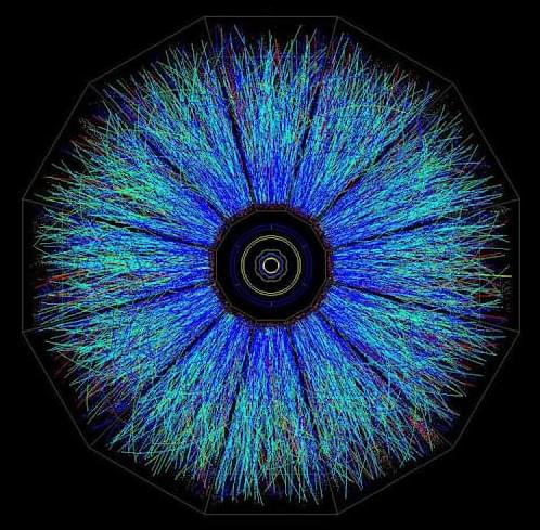
The Relativistic Heavy Ion Accelerator (RHIC), from the Brookhaven Laboratory in the United States, is a sophisticated device capable of accelerating gold ions to a speed of up to 99.995% that of light. Thanks to him, it has recently been possible to verify, for example, Einstein’s famous equation E=mc2.


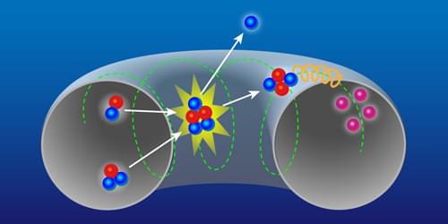
The observation of self-heating in magnetically confined plasmas represents a milestone on the road to fusion reactors based on such plasmas.
A fusion reactor would generate electricity using the energy released by nuclear-fusion reactions occurring in a plasma. A key step in the race toward realizing the dream of such a reactor is the creation of a burning plasma—one in which the fusion reactions themselves supply most of the heating needed to keep the plasma at fusion-relevant temperatures. This step has recently been demonstrated for inertially confined plasmas [1, 2] (see Research News: Ignition First in a Fusion Reaction) but has so far remained elusive for magnetically confined ones. This goal could now be within reach thanks to direct evidence for fusion-induced heating of electrons in magnetically confined plasmas obtained by Vasily Kiptily and colleagues at the UK-based Joint European Torus (JET) facility [3].
The fusion of two heavy hydrogen isotopes—deuterium (D) and tritium (T)—presents the most promising path to a fusion reactor, both because of the relative ease in getting these isotopes to fuse and because of the large amount of energy released in each reaction. When D and T fuse, an alpha particle (a helium-4 nucleus) and a neutron are generated, carrying the released energy in the form of kinetic energy. The goal of achieving energy production from controlled fusion on Earth relies on the created alpha particles remaining in the plasma and heating the fusion fuel to keep the reactions going, while the kinetic energy of neutrons escaping the plasma is converted to electrical energy.

Classical thermodynamics has only a handful of laws, of which the most fundamental are the first and second. The first says that energy is always conserved; the second law says that heat always flows from hot to cold. More commonly this is expressed in terms of entropy, which must increase overall in any process of change. Entropy is loosely equated with disorder, but the Austrian physicist Ludwig Boltzmann formulated it more rigorously as a quantity related to the total number of microstates a system has: how many equivalent ways its particles can be arranged.
The second law appears to show why change happens in the first place. At the level of individual particles, the classical laws of motion can be reversed in time. But the second law implies that change must happen in a way that increases entropy. This directionality is widely considered to impose an arrow of time. In this view, time seems to flow from past to future because the universe began — for reasons not fully understood or agreed on — in a low-entropy state and is heading toward one of ever higher entropy. The implication is that eventually heat will be spread completely uniformly and there will be no driving force for further change — a depressing prospect that scientists of the mid-19th century called the heat death of the universe.
Boltzmann’s microscopic description of entropy seems to explain this directionality. Many-particle systems that are more disordered and have higher entropy vastly outnumber ordered, lower-entropy states, so molecular interactions are much more likely to end up producing them. The second law seems then to be just about statistics: It’s a law of large numbers. In this view, there’s no fundamental reason why entropy can’t decrease — why, for example, all the air molecules in your room can’t congregate by chance in one corner. It’s just extremely unlikely.

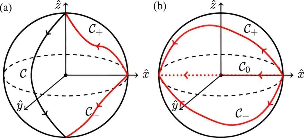
A potentially game-changing theoretical approach to quantum computing hardware avoids much of the problematic complexity found in current quantum computers. The strategy implements an algorithm in natural quantum interactions to process a variety of real-world problems faster than classical computers or conventional gate-based quantum computers can.
“Our finding eliminates many challenging requirements for quantum hardware,” said Nikolai Sinitsyn, a theoretical physicist at Los Alamos National Laboratory. He is co-author of a paper on the approach in the journal Physical Review A. “Natural systems, such as the electronic spins of defects in diamond, have precisely the type of interactions needed for our computation process.”
Sinitsyn said the team hopes to collaborate with experimental physicists also at Los Alamos to demonstrate their approach using ultracold atoms. Modern technologies in ultracold atoms are sufficiently advanced to demonstrate such computations with about 40 to 60 qubits, he said, which is enough to solve many problems not currently accessible by classical, or binary, computation. A qubit is the basic unit of quantum information, analogous to a bit in familiar classical computing.

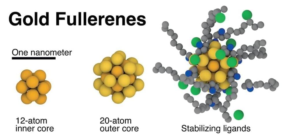
Rice University chemists have discovered that tiny gold “seed” particles, a key ingredient in one of the most common nanoparticle recipes, are one and the same as gold buckyballs, 32-atom spherical molecules that are cousins of the carbon buckyballs discovered at Rice in 1985.
Carbon buckyballs are hollow 60-atom molecules that were co-discovered and named by the late Rice chemist Richard Smalley. He dubbed them “buckminsterfullerenes” because their atomic structure reminded him of architect Buckminster Fuller’s geodesic domes, and the “fullerene” family has grown to include dozens of hollow molecules.
In 2019, Rice chemists Matthew Jones and Liang Qiao discovered that golden fullerenes are the gold “seed” particles chemists have long used to make gold nanoparticles. The find came just a few months after the first reported synthesis of gold buckyballs, and it revealed chemists had unknowingly been using the golden molecules for decades.

The protons and neutrons making up atomic nuclei are made up of a trio of even smaller fundamental particles known as quarks.
A new study has now mapped out in unprecedented detail the distribution of the different kinds of quark inside a proton, expanding on our understanding of this all-important part of an atom.
Although the quantum landscape within protons is a seething mess of quarks and their opposing antiquarks popping in and out of existence, there is a general dominance of two ‘flavors’ over the others; two up-flavor quarks and a single down-flavor quark.