The National Nanotechnology Initiative promised a lot. It has delivered more.
facebook Share on Facebook Share on Twitter Share via Email.

The National Nanotechnology Initiative promised a lot. It has delivered more.
facebook Share on Facebook Share on Twitter Share via Email.
😳!
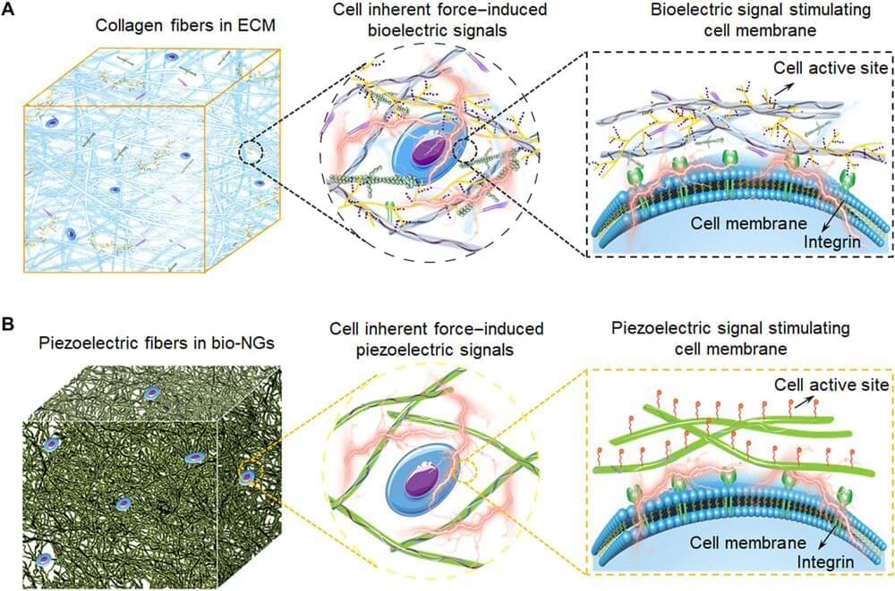
The extracellular matrix (ECM) including three-dimensional (3D) network and bioelectricity can profoundly influence cell development, migration, and functional expression. In a new report now published on Science Advances, Tong Li and a research team in chemistry, nanotechnology, bioelectronics and advanced materials in China, developed an electromechanical coupling bio-nanogenerator abbreviated bio-NG inspired by biophysical cues of the extracellular matrix. The device contained highly discrete piezoelectric fibers to generate piezo potential of up to millivolts to provide in situ electrical stimulation for living cells.

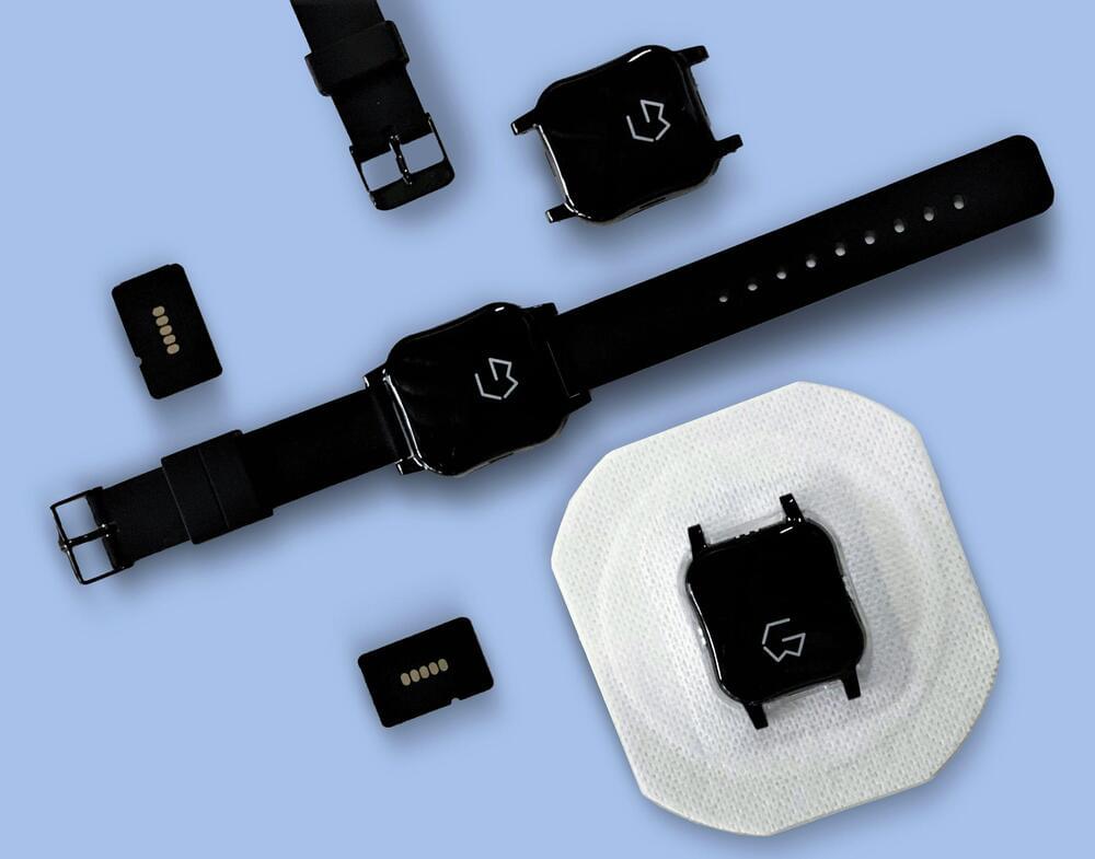
GraphWear, a company pursuing needle-free approaches to glucose monitoring, has closed a $20.5 million Series B round. This Series B round is a vote of confidence by investors in GraphWear’s approach: to monitor key metrics in the body, like glucose, without breaking the skin at all.
GraphWear Technologies was founded in 2015 by Rajatesh Gudibande and Saurabh Radhakrishnan, who had both completed master’s degrees in nanotechnology at the University of Pennsylvania. Specifically, GraphWear is developing a skin-surface-level wearable made of graphene (more on this material later). The sensor is small, about the size of an Apple Watch — but the key piece of technology is actually housed on the bottom. It’s a thin slice of graphene that fits onto the back of the watch, or onto a sticker that can be worn on the abdomen.
This Series B round, says Gudibande, will be focused on helping the company build upon previous validation studies of the wearable, completing a pivotal trial and submitting for FDA clearance. The round was led by Mayfield, with participation from MissionBio Capital, Builders VC and VSC Ventures.
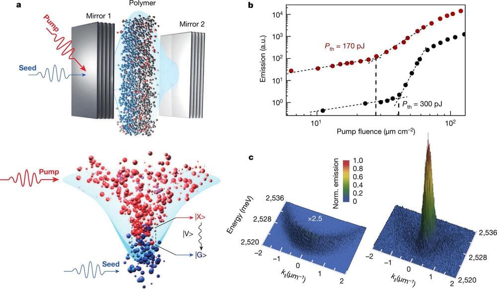
Nonlinearity induced by a single photon is desirable because it can drive power consumption of optical devices to their fundamental quantum limit, and is demonstrated here at room temperature.
The recent progress in nanotechnology1,2 and single-molecule spectroscopy3–5 paves the way for emergent cost-effective organic quantum optical technologies with potential applications in useful devices operating at ambient conditions. We harness a π-conjugated ladder-type polymer strongly coupled to a microcavity forming hybrid light–matter states, so-called exciton-polaritons, to create exciton-polariton condensates with quantum fluid properties. Obeying Bose statistics, exciton-polaritons exhibit an extreme nonlinearity when undergoing bosonic stimulation6, which we have managed to trigger at the single-photon level, thereby providing an efficient way for all-optical ultrafast control over the macroscopic condensate wavefunction. Here, we utilize stable excitons dressed with high-energy molecular vibrations, allowing for single-photon nonlinear operation at ambient conditions.
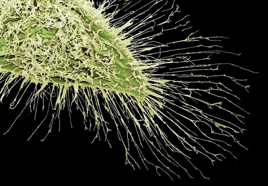
A DNA robot that can walk across biological cell membranes is the first one that can control living cells’ behaviour. The researchers who made the robot hope that it could improve cell-based precision medicine.
A team led by Hong-Hui Wang and Zhou Nie from Hunan University, China, has created a synthetic molecular robot that walks along the outer membrane of biological cells. The robot, powered by an enzyme’s catalytic activity, traverses across receptors that act as stepping stones on the cell surface. With each step, the robot activates a signal pathway that regulates cell migration. Driven by the robot’s movement, the cells can reach speeds of 24 μm/hour.
The researchers write that the DNA robot offers, for the first time, an opportunity to accurately and predictably control the nanoscale operations that power a live cell. They suggest that similar molecular machines that guide cell behaviours could play a role in cell-based therapies and regenerative medicine.

Circa 2012
Faraday and Dirac constructed magnetic monopoles using the practical and mathematical tools available to them. Now physicists have engineered effective monopoles by combining modern optics with nanotechnology. Part matter and part light, these magnetic monopoles travel at unprecedented speeds.
In classical physics (as every student should know) there are no sources or sinks of magnetic field, and hence no magnetic monopoles. Even so, a tight bundle of magnetic flux — such as that created by a long string of magnetic dipoles — has an apparent source or sink at its end. If we map the lines of force with a plotting compass, we think we see a magnetic monopole as our compass cannot enter the region of dense flux. In 1,821 Michael Faraday constructed an effective monopole of this sort by floating a long thin bar magnet upright in a bowl of mercury, with the lower end tethered and the upper end free to move like a monopole in the horizontal plane.

Researchers at MIT have developed a way of quickly changing the magnetic polarity of a ferrimagnet 180 degrees, using just a small applied voltage. According to the researchers, the discovery could herald a new era of ferrimagnetic logic and data storage systems.
The findings were published in the journal Nature Nanotechnology in a paper co-authored by postdoctoral researcher Mantao Huang, MIT professor of materials science and technology Geoffrey Beach, and professor of nuclear science and technology Bilge Yildiz, as well as 15 other researchers from MIT and other institutions in Minnesota, Germany, Spain, and Korea.
The majority of magnets we come across are of “ferromagnetic” materials. The atoms in these materials are oriented in the same direction with their north-south magnet axes; thus, their combined strength is strong enough to create attraction. As a result, these materials are often used in the modern high-tech environment.
A sperm’s task may appear straightforward; after all, all it needs to do is swim to an egg and insert genetic material. However, in some cases, a healthy sperm’s inability to swim may result in infertility, which affects around 7 percent of all males.
This condition is called asthenozoospermia, and there is currently no cure. However, one study conducted in 2016 and published in the journal Nano Letters has set the example for what could be possible in the future: A team of researchers from the Institute for Integrative Nanosciences at IFW Dresden in Germany developed tiny motors that can make sperm swim better as they make their way to an egg, essentially acting as a taxi.
These so-called “spermbots” basically consist of a tiny micromotor, which is basically a spiraling piece of metal that wraps around the sperm’s tail. Serving as an “on-board power supply”, the motor navigates the sperm via a magnetic field, helping the sperm swim to the egg with ease. When the sperm makes contact with the egg for fertilization, the motor slips right off, and the magnetic field doesn’t harm any of the cells involved, making it ideal for usage on living tissue, according to the researchers.

Using specialized nanoparticles embedded in plant leaves, MIT engineers have created a novel light-emitting plant that can be charged by an LED. In this image, the green parts are the nanoparticles that have been aggregated on the surface of spongy mesophyll tissue within the plant leaves. Credit: Courtesy of the researchers.
Using nanoparticles that store and gradually release light, engineers create light-emitting plants that can be charged repeatedly.
Using specialized nanoparticles embedded in plant leaves, MIT.