Magnetic random-access memories (MRAMs) are data storage devices that store digital data within nanomagnets, representing it in binary code (i.e., as “0” or “1”). The magnetization of nanomagnets inside these memory devices can be directed upward or downward.
Over the past decade, electronics engineers have introduced techniques that can switch this direction using in-plane electrical currents. These techniques ultimately enabled the creation of a new class of MRAM devices, referred to as spin-orbit torque (SOT)-MRAMs.
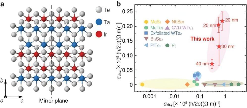
While existing techniques to switch magnetization direction of nanomagnets in SOT-MRAMs have proved effective, many only work if external magnetic fields are aligned with the direction of the electric current. In a recent paper published in Nature Electronics, researchers at the National University of Singapore demonstrated the field-free switching of the perpendicular magnetic anisotropy (PMA) ferromagnet cobalt iron boron (CoFeB) at ambient conditions.
