RED Digital Cinema has announced its first Android phone featuring the world’s first glasses-free holographic display.


ELF emmit is the world’s first wearable mind stimulating headband, based on pulsed electromagnetic technology. Operates in five different modes: Sleep, Anti-stress, Superlearning, Concentrate, Meditate. Designed to assist you in every area of life. Powered by smart phone or tablet. Operated by free mobile application.
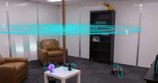
It seems like almost everything has gone wireless. Yet somehow, when it comes to charging electronic devices, we still have to deal with cords. Sure wireless charging exists, but only for small devices like your smartphone. And even then, it’s not convenient as you might hope. To actually power a device, a phone must maintain contact with a charging pad, which means it can’t be used while charging. This seems to be even a bigger hassle than dealing with cords and cables.

Wireless charging is a great idea in theory: You can just place your device on a charging mat without having to mess with any wires. But it still doesn’t solve the main hassle of charging in the first place, which is the requirement to leave your device in one place. But now, scientists may have found the answer to that problem using principles from quantum mechanics.
Currently, wireless, or inductive, charging uses an electromagnetic field to transmit energy over very short distances. That’s why your phone, or whatever device you’re charging wirelessly, must remain near a wireless pad in order to actually charge. But Shanhui Fan and his team at Stanford University have published an article in Nature that details a wireless charging system that works even when the charger and device are a meter apart. You can also move around the device while it’s being charged without interrupting the power transfer.
It works by using a principle of quantum mechanics called parity-time symmetry to create a charger with a self-adjusting power flow. A connected amplifier automatically controls the flow of power between the transmitter and receiver. As a device moves further away from the charger, the power levels adjust automatically to ensure an even and uninterrupted flow of current.
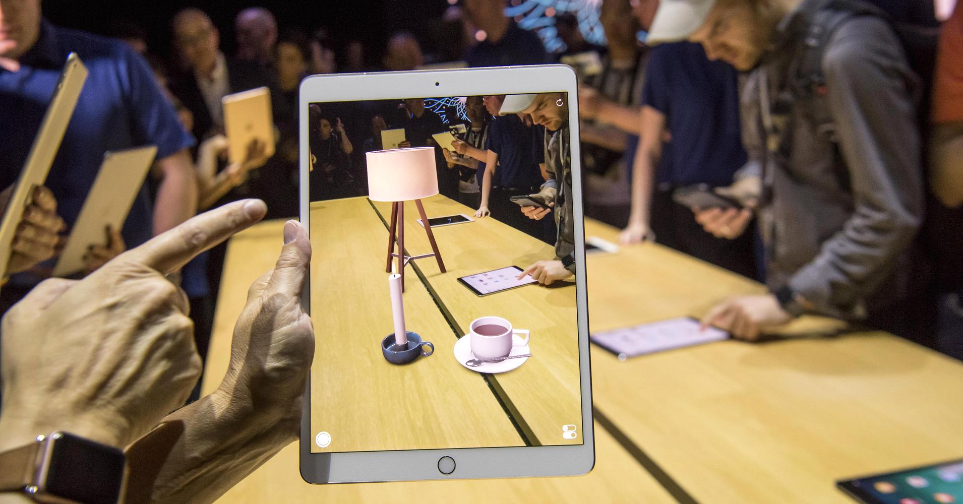
One of Apple’s new announcements has tech experts excited for augmented reality. One chief executive calls it a “game-changer.”
Apple unveiled its new operating system for its iPhone and iPad products, the iOS 11, at the Apple Worldwide Developers Conference on Monday.
The system also introduces ARKit, a new framework for developers to more easily build apps that use augmented reality: the tech that allows devices to display computer-generated images over the real world.
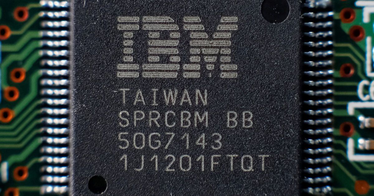
Who said Moore’s Law was dead? Certainly not IBM or its chip partners Globalfoundries and Samsung. The trio has developed a transistor manufacturing process that should pave the way for 5-nanometer chips. While the team etched the chip using the same extreme ultraviolet lithography (EUV) used for the breakthrough 7nm chip, it ditched the common FinFET (fin field effect) transistor design in favor of stacks of silicon nanosheets. The switch makes it possible to fine-tune individual circuits to maximize their performance as they’re crammed into an incredibly small space. How small? At 5nm, the group says it can squeeze 30 billion transistors into a chip the size of a fingernail (see below) — not bad when the 7nm chip held 20 billion transistors a couple of years ago.
IBM sees the technique helping its own cognitive computing efforts as well as the Internet of Things and other “data-intensive” tasks. However, it’s also painting a rosy picture for the future of mobile devices — it imagines phones having “two to three times” more battery life than current devices. That’s likely optimistic (phone makers tend to focus on speed over longevity), but it won’t be shocking if future hardware is both faster and wrings out a little more from every charge.
Just don’t expect to see real-world examples of this for a while. We haven’t even seen devices shipping with 7nm chips (they’re not expected until 2018 at the earliest), so it could easily be a couple of years or more before 5nm arrives. Still, that 5nm is even on the roadmap is important. Chip designers won’t have to reinvent the wheel to get meaningful improvements, and you won’t have to worry about device performance growing stale for at least the next few years.
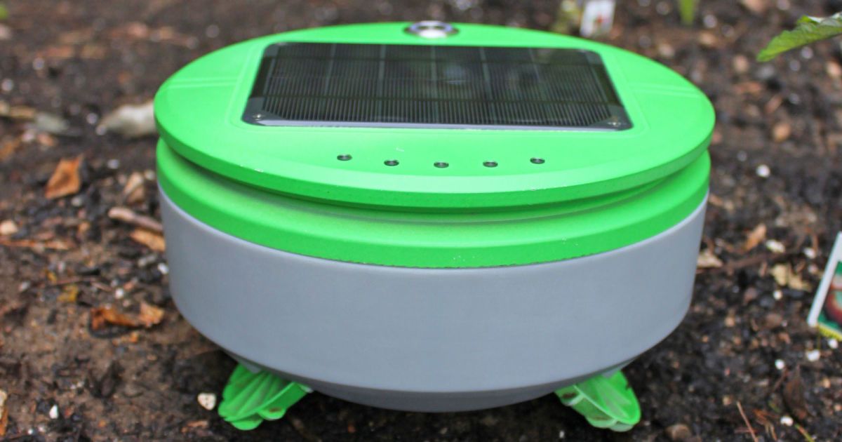
Let’s be honest: while planting your garden can be fun, weeding it usually isn’t. Not unless you enjoy crouching down for long stretches, anyway. You might not have to endure the drudgery for too much longer, though. Roomba co-creator Joe Jones and Franklin Robotics are launching Tertill, a robot that weeds your garden all by itself. The machine automatically roams the soil, using sensors to identify small plants (you use collars to protect young crops) and chop them down. It’s solar-powered, so you don’t have to dock it — you can even leave it out in the rain.
In addition to pairing with your phone through Bluetooth, the machine has a USB port to charge during particularly gloomy weeks.
The design does require some careful planning to work properly. You need to space your crops loosely so that the robot can kill weeds in between, and you’ll want to avoid any steep inclines so Tertill doesn’t stuck. There will have to be some kind of basic barrier to prevent the vehicle from wandering away, too. You may also have to rethink how you kill weeds. While you’re probably used to pulling weeds out by the roots, Franklin is counting on its bot repeatedly cutting down weeds until they wither and die.

IBM, its Research Alliance partners Globalfoundries and Samsung, and equipment suppliers have developed an industry-first process to build silicon nanosheet transistors that will enable 5 nanometer (nm) chips. The details of the process will be presented at the 2017 Symposia on VLSI Technology and Circuits conference in Kyoto, Japan. In less than two years since developing a 7nm test node chip with 20 billion transistors, scientists have paved the way for 30 billion switches on a fingernail-sized chip.
The resulting increase in performance will help accelerate cognitive computing, the Internet of Things (IoT), and other data-intensive applications delivered in the cloud. The power savings could also mean that the batteries in smartphones and other mobile products could last two to three times longer than today’s devices, before needing to be charged.
Scientists working as part of the IBM-led Research Alliance at the SUNY Polytechnic Institute Colleges of Nanoscale Science and Engineering’s NanoTech Complex in Albany, NY achieved the breakthrough by using stacks of silicon nanosheets as the device structure of the transistor, instead of the standard FinFET architecture, which is the blueprint for the semiconductor industry up through 7nm node technology.
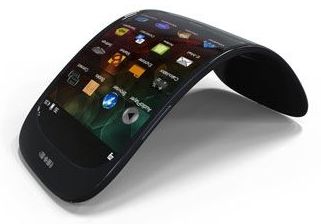
A smartphone touchscreen is an impressive piece of technology. It displays information and responds to a user’s touch. But as many people know, it’s easy to break key elements of the transparent, electrically conductive layers that make up even the sturdiest rigid touchscreen. If flexible smartphones, e-paper and a new generation of smart watches are to succeed, they can’t use existing touchscreen technology.
Your smartphone can’t do this – yet. (Image: Peter Sobolev)

This is the age of the citizen journalist where people on the street armed with a smartphone and a Twitter account are often the first on the scene of an accident, fire or other emergency. These folks know about an incident that requires emergency services well before first responders.
Dataminr introduced a new product on stage at TechCrunch Disrupt today in New York City that searches the Twitter firehose for emergency situations throughout the city, and channels news alerts to first responders.
The system is designed to filter out fake announcements, jokesters, pranksters and other non events, so first responders aren’t wasting their time chasing rumors of non-events.