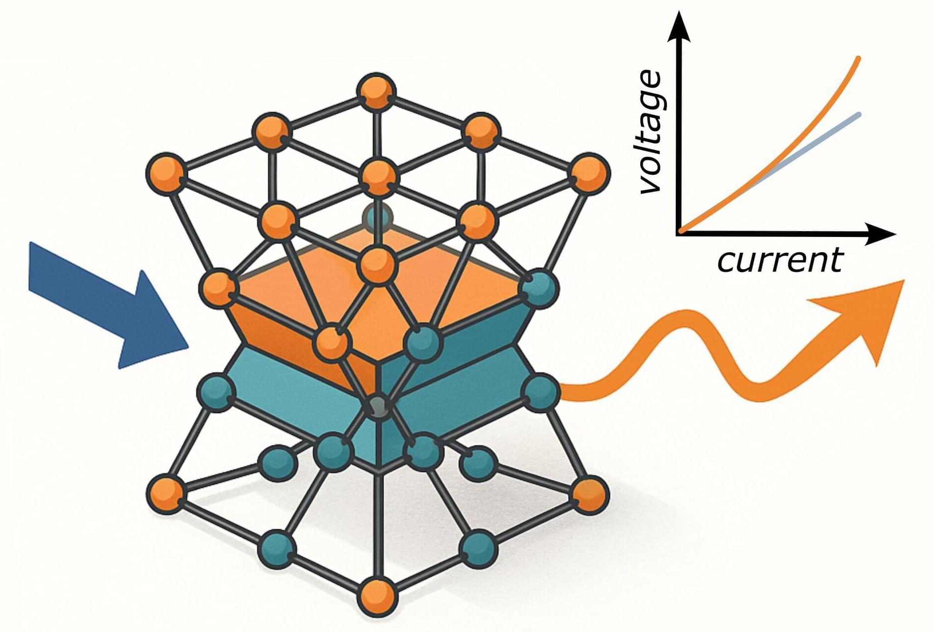
Oxygen evolution is considered one of the most energy-intensive steps in water electrolysis and is therefore a key factor for more efficient green hydrogen production. Modeling of the reaction mechanisms has so far been based on the assumption that the elementary steps take place sequentially and not in a concerted manner.
A team led by Prof. Dr. Kai S. Exner from the University of Duisburg-Essen has now shown that this assumption is not always correct. The results, published in Nature Communications, open up new possibilities for improving solid catalysts for energy conversion and storage applications.
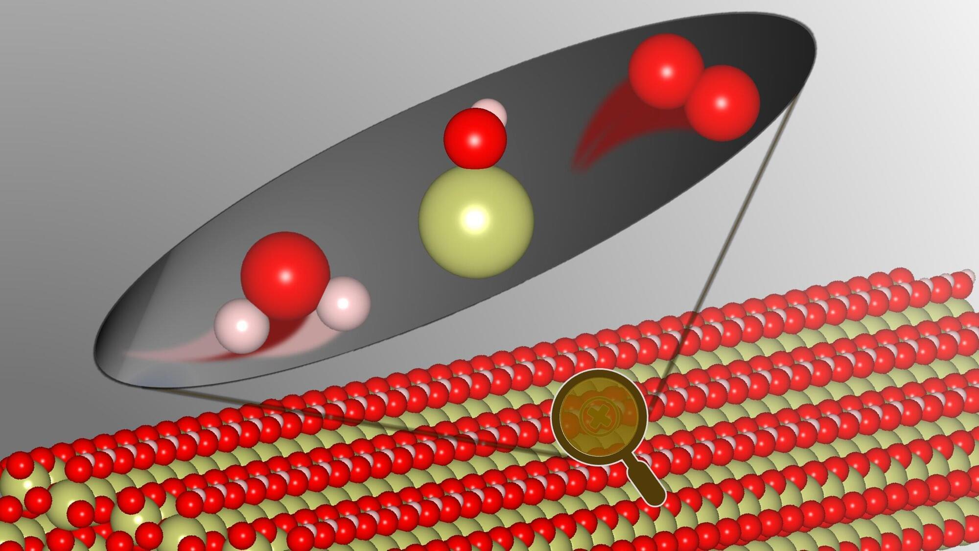
There are two basic types of catalysis: homogeneous catalysts have the same physical state as the substances being converted (e.g., they all are liquid), while heterogeneous catalysts are in a different phase, for example a solid that reacts with liquids or gases. For a reaction to take place on the surface of a solid catalyst, the starting materials (reactants) must attach to its surface (adsorption) and then dissolve again after the reaction has taken place (desorption).