Almost 200 million people, including children, around the world have endometriosis, a chronic disease in which the lining of the uterus grows outside of the uterus. More severe symptoms, such as extreme pain and potentially infertility, can often be mitigated with early identification and treatment, but no single point-of-care diagnostic test for the disease exists despite the ease of access to the tissue directly implicated.
While Penn State Professor Dipanjan Pan said that the blood and tissue shed from the uterus each month is often overlooked—and even stigmatized by some—as medical waste, menstrual effluent could enable earlier, more accessible detection of biological markers to help diagnose this disease.
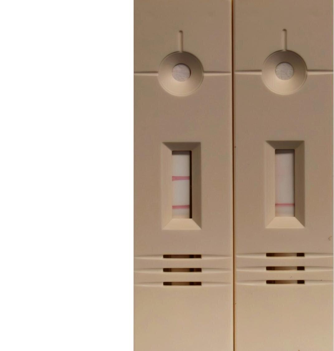
Pan and his group have developed a proof-of-concept device capable of detecting HMGB1, a protein implicated in endometriosis development and progression, in menstrual blood with 500% more sensitivity than existing laboratory approaches. The device, which looks and operates much like a pregnancy test in how it detects the protein, hinges on a novel technique to synthesize nanosheets made of the atomically thin 2D material borophene, according to Pan, the Dorothy Foehr Huck & J. Lloyd Huck Chair Professor in Nanomedicine and corresponding author of the study detailing the team’s work.