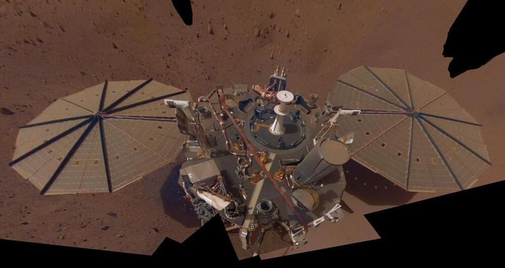
Menu

Blog

Archive for the ‘materials’ category: Page 256

Oct 7, 2015

#18 Avatar Technology Digest / Paralyzed Patients Control Comp…

Posted by in categories: 3D printing, bioengineering, biotech/medical, computing, materials, robotics/AI

1. A heart of foam.
2. Artificial arteries.
3. Brain implants.
4. Robotic hand that can recognize objects by Feel.
5. Upside-Down Rover to explore Europa.


Welcome to #18 Avatar Technology Digest. Again, get ready for exciting news on Technology, Medical Cybernetics and Artificial Intelligence. Thank you for watching us. You are welcome to Subscribe, follow us in social media, leave your comments and join the conversation. And here are the top stories of the last week.

1) A heart of foam could replace your own. Existing artificial hearts have multiple moving parts, which increases the chance of failure, but this new device is just a single piece of material. Researchers inspired by soft robots have built a pumping artificial heart that could one day replace the real deal.
The team of Bioengineers at Cornell University build their robots out of a solid, plastic foam, which naturally has an interconnected network of tubes to let air flow – just as our muscles are permeated by blood vessels. A solid coating of plastic seals everything inside like a skin.

Continue reading “#18 Avatar Technology Digest / Paralyzed Patients Control Comp…” »

Oct 5, 2015

Australian engineers just built a quantum logic gate in silicon for the first time

Posted by in categories: computing, materials, particle physics, quantum physics

For decades, researchers have been trying to build a computer that harnesses the enormous potential of quantum mechanics. Now engineers from the University of New South Wales (UNSW) in Australia have overcome the final hurdle, by creating a quantum logic gate in silicon — the same material that today’s computer chips are made from.

The newly developed device allows two quantum bits — or qubits — to communicate and perform calculations together, which is a crucial requirement for quantum computers. Even better, the researchers have also worked out how to scale the technology up to millions of qubits, which means they now have the ability to build the world’s first quantum processor chip and, eventually, the first silicon-based quantum computer.

Continue reading “Australian engineers just built a quantum logic gate in silicon for the first time” »

Oct 1, 2015

Graphene nanoribbons as electronic highways

Posted by in categories: materials, physics, solar power, sustainability

Physicists have developed a method to synthesise a unique and novel type of material which resembles a graphene nanoribbon but in molecular form. This material could be important for the further development of organic solar cells.

Read more

Oct 1, 2015

IBM unlocks the secret to carbon nanotube transistors

Posted by in categories: computing, engineering, internet, materials, neuroscience

Following Moore’s law is getting harder and harder, especially as existing components reach their physical size limitations. Parts like silicon transistor contacts — the “valves” within a transistor that allow electrons to flow — simply can’t be shrunken any further. However, IBM announced a major engineering achievement on Thursday that could revolutionize how computers operate: they’ve figured out how to swap out the silicon transistor contacts for smaller, more efficient, carbon nanotubes.

The problem engineers are facing is that the smaller silicon transistor contacts get, the higher their electrical resistance becomes. There comes a point where the components simply get too small to conduct electrons efficiently. Silicon has reached that point. But that’s where the carbon nanotubes come in. These structures measure less than 10 nanometers in diameter — that’s less than half the size of today’s smallest silicon transistor contact. IBM actually had to devise a new means of attaching these tiny components. Known as an “end-bonded contact scheme” the 10 nm electrical leads are chemically bonded to the metal substructure. Replacing these contacts with carbon nanotubes won’t just allow for computers to crunch more data, faster. This breakthrough ensures that they’ll continue to shrink, following Moore’s Law, for several iterations beyond what silicon components are capable of.

“These chip innovations are necessary to meet the emerging demands of cloud computing, Internet of Things and Big Data systems,” Dario Gil, vice president of Science & Technology at IBM Research, said in a statement. “As technology nears the physical limits of silicon, new materials and circuit architectures must be ready to deliver the advanced technologies that will drive the Cognitive Computing era. This breakthrough shows that computer chips made of carbon nanotubes will be able to power systems of the future sooner than the industry expected.” The study will be formally published October 2nd, in the journal Science. This breakthrough follows a number of other recent minimization milestones including transistors that are only 3-atoms thick or constructed from a single atom.

Read more

Sep 30, 2015

Pushing computers towards petahertz, with femtosecond lasers and weird dielectrics

Posted by in categories: computing, electronics, materials, quantum physics

New findings published by quantum scientists in Germany could pave the way towards computer chips that use light instead of electricity to control their internal logic. Where today’s silicon-based electrical computer chips are capable of speeds in the gigahertz range, the German light-based chips would be some 1,000,000 times faster, operating in the petahertz range.

Rather than focusing on an exciting new semiconductor, or some metamaterial that manipulates light in weird and wonderful ways, this research instead revolves around dielectrics. In the field of electronics, materials generally fall into one of three categories: charge carriers (conductors), semiconductors, and dielectrics (insulators). As the name suggests, a semiconductor only conduct electricity some of the time (when it receives a large enough jolt of energy to get its electrons moving). In a dielectric, the electrons are basically immobile, meaning electricity can’t flow across them. Apply too much energy, and you destroy the dielectric. As a general rule, there’s no switching: A dielectric either insulates, or it breaks.

Basically, the Max Planck Institute and Ludwig Maximilian University in Germany have found that dielectrics, using very short bursts of laser light, can be turned into incredibly fast switches. The researchers took a small triangle of silica glass (a strong insulator), and then coated two sides with gold, leaving a small (50nm) gap in between (see below). By shining a femtosecond infrared laser at the gap, the glass started conducting and electricity flowed across the gap. When the laser is turned off, the glass becomes an insulator again.

Read more

Sep 30, 2015

3D printing in gel shows how scientists could print human organs

Posted by in categories: 3D printing, biotech/medical, cyborgs, materials, neuroscience, transhumanism

While scientists have had success in the past printing structures like “bionic ears,” a clear path to making functional internal organs and tissue hasn’t really emerged. However, researchers at the University of Florida in Gainesville have developed a way of printing complex objects in gel, a method that could help pave the way to 3D-printed organs in the future.

The hard thing about printing intricate organic structures like blood vessels and complicated organs is that they collapse under their own weight before they solidify. The gel here, which is made of an acrylic acid polymer, acts as a scaffold to hold the structure in place during the printing process. That approach has already allowed the team to print with organic materials — and even make a replica of a human brain.

Continue reading “3D printing in gel shows how scientists could print human organs” »

Sep 28, 2015

New hydrogel can keep stem cells alive for heart repair

Posted by in categories: biotech/medical, materials

A new hydrogel protects stem cells inside the body, making existing therapies a lot more effective.

Read more

Sep 24, 2015

‘4-D’ printing technology allows self-folding of complex ‘transformer’ objects, using smart shape-memory materials

Posted by in categories: 4D printing, materials

This image shows the self-folding process of smart shape-memory materials with slightly different responses to heat. Using materials that fold at slightly different rates ensures that the components do not interfere with one another during the process. (credit: Qi Laboratory)

Using components made from smart shape-memory materials (which can return to their original shape) with slightly different responses to heat, researchers have demonstrated a “four-dimensional” printing technology that allows for creating complex, self-folding structures.

Read more

Sep 23, 2015

Permanent data storage with light

Posted by in categories: computing, materials, nanotechnology

The first all-optical permanent on-chip memory has been developed by scientists of Karlsruhe Institute of Technology (KIT) and the universities of Münster, Oxford, and Exeter. This is an important step on the way towards optical computers. Phase change materials that change their optical properties depending on the arrangement of the atoms allow for the storage of several bits in a single cell. The researchers present their development in the journal Nature Photonics (10.1038/nphoton.2015.182).

Light determines the future of information and communication technology: With optical elements, computers can work more rapidly and more efficiently. Optical fibers have long since been used for the transmission of data with light. But on a computer, data are still processed and stored electronically. Electronic exchange of data between processors and the memory limits the speed of modern computers. To overcome this so-called von Neumann bottleneck, it is not sufficient to optically connect memory and processor, as the optical signals have to be converted into electric signals again. Scientists, hence, look for methods to carry out calculations and data storage in a purely optical manner.

Scientists of KIT, the University of Münster, Oxford University, and Exeter University have now developed the first all-optical, non-volatile on-chip memory. “Optical bits can be written at frequencies of up to a gigahertz. This allows for extremely quick data storage by our all-photonic memory,” Professor Wolfram Pernice explains. Pernice headed a working group of the KIT Institute of Nanotechnology (INT) and recently moved to the University of Münster. “The memory is compatible not only with conventional optical fiber data transmission, but also with latest processors,” Professor Harish Bhaskaran of Oxford University adds.

Read more

Sep 22, 2015

Physicists Discovered New State of Matter

Posted by in categories: materials, particle physics, quantum physics

I remember the time when states of matter were pretty simple: Solid, liquid and gas. Then came plasma state, supercritical fluid, Bose –Einstein condensate and more. Now this list of states of matter has grown by one more, with the surprising discovery of a new state dubbed “dropletons” that shows some similarity to liquids but occur under very unlike circumstances.

The discovery of new state of matter occurred when a team of scientists at the University of Colorado Joint Institute for Lab Astrophysics were concentrating laser light on gallium arsenide (GaAs) to generate excitons.

Excitons are made when a photon strikes a material, mostly a semiconductor. If an electron is knocked loose, or excited, it leaves what is labelled as “electron hole” behind. If the forces of other charges at very close distance keep the electron close enough to the hole in order to feel an attraction, a certain state forms called as an Exciton. Excitons are also called quasiparticles because the holes and electrons act together as if they were like a single particle.

Read more