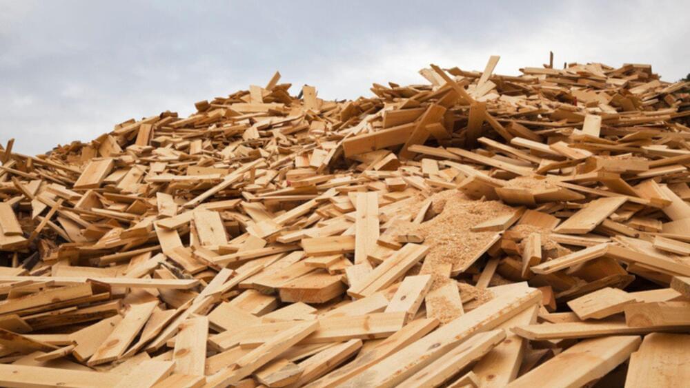
David Fischer, an MIT Energy Fellow at the Plasma Science and Fusion Center, is observing ways irradiation damages thin high-temperature superconductor tapes in the design of ARC, a fusion pilot plant concept.
Category: materials – Page 210
Superconductivity is a phenomenon where an electric circuit loses its resistance and becomes extremely efficient under certain conditions. There are different ways in which this can happen which were thought to be incompatible. For the first time, researchers discover a bridge between two of these methods to achieve superconductivity. This new knowledge could lead to a more general understanding of the phenomena, and one day to applications.
If you’re like most people, there are three states of matter in your everyday life: solid, liquid, and gas. You might be familiar with a fourth state of matter called plasma, which is like a gas that got so hot all its constituent atoms came apart, leaving behind a super hot mess of subatomic particles. But did you know about a so-called fifth state of matter at the complete opposite end of the thermometer? It’s known as a Bose-Einstein condensate (BEC).
“A BEC is a unique state of matter as it is not made from particles, but rather waves,” said Associate Professor Kozo Okazaki from the Institute for Solid State Physics at the University of Tokyo. “As they cool down to near absolute zero, the atoms of certain materials become smeared out over space. This smearing increases until the atoms — now more like waves than particles — overlap, becoming indistinguishable from one another. The resulting matter behaves like it’s one single entity with new properties the preceding solid, liquid or gas states lacked, such as superconduction. Until recently superconducting BECs were purely theoretical, but we have now demonstrated this in the lab with a novel material based on iron and selenium (a nonmetallic element).”
OverviewDefeXtiles are thin, flexible textiles of many materials that can quickly be printed into a variety of 3D forms using an inexpensive, unmodified, 3D printer with no additional software.
A team of researchers from China, Spain, Russia and Portugal has developed a way to use Moiré lattices to optically induce and highlight the formation of optical solitons under different geometrical conditions. In their paper published in the journal Nature Photonics, the group describes their work, which involved using photorefractive nonlinear media as a means of localizing laser light into tight spots.
Solitons are quasiparticles propagated by a traveling wave. Unlike waves such as those produced in water, solitons are neither followed nor preceded by other such waves—they also hold their shape as they move. They are important because they are able to prevent diffraction from occurring, which is why they play such an important role in telecommunications and other information carrier systems. Moiré lattices are patterns that sometimes emerge in printed or scanned images when two patterns overlap one another in an offset fashion. They have been used in graphene-based research efforts and work that involves manipulating very cold atoms. They have also been found to play a roll in the development of colloidal clusters.
In this new work, the researchers were investigating the ways that light could be stopped from spreading—more specifically, ways that laser light could be trapped in a tight spot. To that end, they used a laser beam to stencil a special a type of crystal: a photorefractive strontium barium niobite crystal with nonlinear holographic properties. The stencil forced a beam of laser light to form into a twisted Moiré lattice. As the light moved through the lattice, the researchers found that solitons formed. They also found that they could adjust the threshold of the laser power by fine-tuning the angles of the twists in the lattice. Additionally, the formation of solitons in the lattices occurred with smooth transitions, from fully periodic geometries to aperiodic ones. The researchers also noted that such thresholds in their setup were quite low.
Nylon might seem the obvious go-to material for electronic textiles—not only is there an established textiles industry based on nylon, but it conveniently has a crystalline phase that is piezoelectric—tap it and you get a build-up of charge perfect for pressure sensing and harvesting energy from ambient motion.
Unfortunately, forming nylon into fibers while getting it to take on the crystal structure that has a piezoelectric response is not straightforward. “This has been a challenge for almost half a century,” explains Kamal Asadi, a researcher at the Max-Planck Institute for Polymer Research, Germany, and professor at the University of Bath, U.K. In a recent Advanced Functional Materials report, he and his collaborators describe how they have now finally overcome this.
The piezoelectric phase of nylon holds appeal not just for electronic textiles but all kinds of electronic devices, particularly where there is demand for something less brittle than the conventional piezoelectric ceramics. However, for decades, the only way to produce nylon with the crystalline phase that has a strong piezoelectric response has been to melt it, rapidly cool it and then stretch it so that it sets into a smectic δ’ phase. This produces slabs typically tens of micrometers thick—far too thick for applications in electronic devices or electronic textiles.
Zeppelins are usually equated with the Hindenburg disaster, but today’s airships use modern materials and some aspire to be as luxurious as superyachts.
If a 3D printer leaves gaps in the plastic that it deposits, it’s usually thought of as an unwanted flaw. Now, however, the process has been harnessed to quickly and cheaply produce pliable polymer textiles.
Ordinarily, commonly used fused deposition modelling (FDM)-type printers create items by extruding successive layers of molten plastic. Once the layers of deposited plastic have cooled and fused together, they form a hardened solid object.
Sometimes, though – due to a flaw in the printer or the programming – not enough plastic is extruded. This is known as under-extrusion, and it results in the finished product being full of small gaps.
The equivalent of as many as 1,300 plastic grocery bags per person is landing in places such as oceans and roadways, according to a new study of U.S. plastic trash.
Circa 2015.
LEDs have come a long ways. From the early 70s when a bulky LED watch cost thousands of dollars to LG’s announcement last month that it had created an OLED TV as thin as a magazine, these glowing little bits of magic have become wonderfully cheap and impossibly small. But guess what: they’re about to get much smaller.
A team scientists from the University of Washington just built the world’s thinnest possible LED for use as a light source in electronics. It’s just three atoms thick. No, not three millimeters. Not three nanometers. Three atoms.
“These are 10,000 times smaller than the thickness of a human hair, yet the light they emit can be seen by standard measurement equipment,” said Jason Ross, a UW materials scientist and graduate student who helped with the research. “This is a huge leap of miniaturization of technology, and because it’s a semiconductor, you can do almost everything with it that is possible with existing, three-dimensional silicon technologies.”
Circa 2018
The world’s first-ever hiking boots to use graphene have been unveiled by The University of Manchester and British brand inov-8.
Building on the international success of their pioneering use of graphene in trail running and fitness shoes last summer, the brand is now bringing the revolutionary technology to a market recently starved of innovation.
Just one atom thick and stronger than steel, graphene has been infused into the rubber of inov-8’s new ROCLITE hiking boots, with the outsoles scientifically proven to be 50% stronger, 50% more elastic and 50% harder wearing.