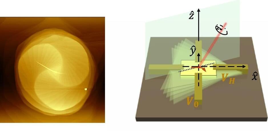
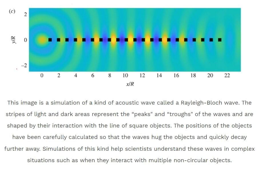
Toggle light / dark theme

Researchers at Purdue University have discovered new waves with picometer-scale spatial variations of electromagnetic fields that can propagate in semiconductors like silicon. The research team, led by Dr. Zubin Jacob, Elmore Associate Professor of Electrical and Computer Engineering and Department of Physics and Astronomy, published their findings in Physical Review Applied in a paper titled “Picophotonics: Anomalous Atomistic Waves in Silicon.”

“The word microscopic has its origins in the length scale of a micron, which is a million times smaller than a meter. Our work is for matter interaction within the picoscopic regime which is far smaller, where the discrete arrangement of atomic lattices changes light’s properties in surprising ways,” says Jacob.

These intriguing findings demonstrate that natural media host a variety of rich light-matter interaction phenomena at the atomistic level. The use of picophotonic waves in semiconducting materials may lead researchers to design new, functional optical devices, allowing for applications in .

face_with_colon_three circa 2020.


Scientists in Australia have developed a new type of electronic material that is touch-responsive and just a fraction of the thickness of current smartphone screens. This could see it one day find use in next-generation mobile devices, and because of its incredible thinness and flexibility, could be manufactured at large scale using roll-to-roll (R2R) processing like a printed newspaper.

The breakthrough comes from researchers at RMIT University, who began with a material commonly used in today’s mobile touchscreens called indium-tin oxide. This transparent material is highly conductive but does have its shortcomings, chiefly that it is very brittle, so the team sought to give it better pliability by greatly reducing its thickness.

“We’ve taken an old material and transformed it from the inside to create a new version that’s supremely thin and flexible,” says lead researcher Dr Torben Daeneke. “You can bend it, you can twist it, and you could make it far more cheaply and efficiently than the slow and expensive way that we currently manufacture touchscreens.”

Circa 2015 face_with_colon_three


MIT physicists have created a superfluid gas, the so-called Bose-Einstein condensate, for the first time in an extremely high magnetic field. The magnetic field is a synthetic magnetic field, generated using laser beams, and is 100 times stronger than that of the world’s strongest magnets. Within this magnetic field, the researchers could keep a gas superfluid for a tenth of a second—just long enough for the team to observe it. The researchers report their results this week in the journal Nature Physics.

A superfluid is a phase of matter that only certain liquids or gases can assume, if they are cooled to extremely low temperatures. At temperatures approaching absolute zero, cease their individual, energetic trajectories, and start to move collectively as one wave.

Superfluids are thought to flow endlessly, without losing energy, similar to electrons in a superconductor. Observing the behavior of superfluids therefore may help scientists improve the quality of superconducting magnets and sensors, and develop energy-efficient methods for transporting electricity.

In an unprecedented experiment, two teams of scientists on either sides of the Atlantic have replicated a material that was previously not produced anywhere on Earth.

As NPR reports, the replication of this powerful compound could have huge implications not just for the manufacturing of high-end machinery, but also for international relations to boot.

Called tetrataenite, the primarily iron-and-nickel compound is normally able to cool for millions of years as it tumbles around in asteroids. As a press release out of the University of Cambridge notes, the researchers who worked in tandem with Boston’s Northeastern University found that if they add phosphorous to the mix, they were able to make synthetic tetrataenite.

When 2D layered materials are made thinner (i.e., at the atomic scale), their properties can dramatically change, sometimes resulting in the emergence of entirely new features and in the loss of others. While new or emerging properties can be very advantageous for the development of new technologies, retaining some of the material’s original properties is often equally important.

Researchers at Tsinghua University, the Chinese Academy of Sciences and the Frontier Science Center for Quantum Information have recently been able to realize tailored Ising superconductivity in a sample of intercalated bulk niobium diselenide (NbSe2), a characteristic of bulk NbSe2 that is typically compromised in . The methods they used, outlined in a paper published in Nature Physics, could pave the way towards the fabrication of 2D thin-layered superconducting materials.

“Atomically thin 2D materials exhibit interesting properties that are often distinct from their bulk materials, which consist of hundreds and thousands of layers,” Shuyun Zhou, one of the researchers who carried out the study, told Phys.org. “However, atomically thin films/flakes are difficult to fabricate, and the emerging new properties are sometimes achieved by sacrificing some other important properties.”

In the effort to efficiently convert heat into electricity, easily accessible materials from harmless raw materials open up new perspectives in the development of safe and inexpensive so-called thermoelectric materials. A synthetic copper mineral acquires a complex structure and microstructure through simple changes in its composition, thereby laying the foundation for the desired properties, according to a study published recently in the journal Angewandte Chemie.

The novel synthetic material is composed of copper, manganese, germanium, and sulfur, and it is produced in a rather simple process, explains materials scientist Emmanuel Guilmeau, CNRS researcher at CRISMAT laboratory, Caen, France, who is the corresponding author of the study. The powders are simply mechanically alloyed by ball-milling to form a precrystallized phase, which is then densified by 600 degrees Celsius.

The Celsius scale, also known as the centigrade scale, is a temperature scale named after the Swedish astronomer Anders Celsius. In the Celsius scale, 0 °C is the freezing point of water and 100 °C is the boiling point of water at 1 atm pressure.