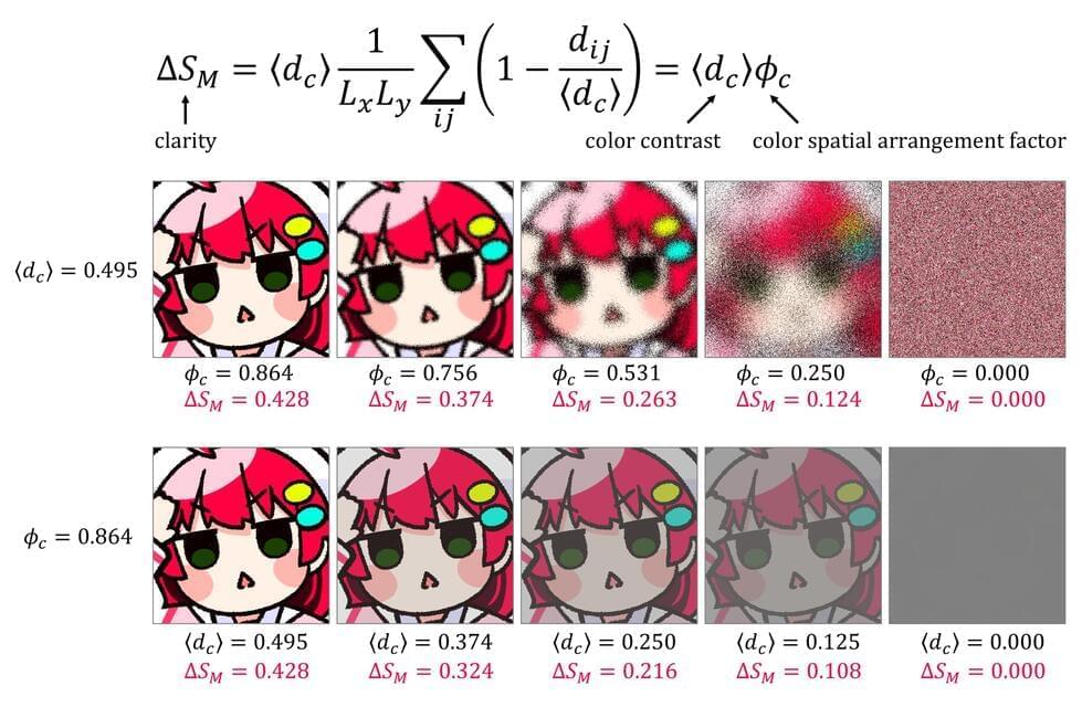
Toggle light / dark theme

Separation processes are essential in the purification and concentration of a target molecule during water purification, removal of pollutants, and heat pumping, accounting for 10–15% of global energy consumption. To make the separation processes more energy efficient, improvement in the design of porous materials is necessary. This could drastically reduce energy costs by about 40–70%. The primary approach to improving the separation performance is to precisely control the pore structure.

In this regard, porous carbon materials offer a distinct advantage as they are composed of only one type of atom and have been well-used for separation processes. They have large pore volumes and surface areas, providing in gas separation, , and storage. However, pore structures generally have high heterogeneity with low designability. This poses various challenges, limiting the applicability of carbon materials in separation and storage.

Now, a team of researchers from Japan, led by Associate Professor Tomonori Ohba from Chiba University and including master’s students, Mr. Kai Haraguchi and Mr. Sogo Iwakami, has fabricated fullerene-pillared porous (FPPG)—a carbon composite comprising nanocarbons—using a bottom-up approach with highly designable and controllable pore structures.

Queen guitarist Brian May and Dante Lauretta, the chief scientist of NASA’s asteroid-sampling OSIRIS-REx mission, have collaborated on a book about the asteroid Bennu — and it’s not a PR stunt.

OSIRIS-REx snagged a sample of Bennu in October 2020 and is currently speeding toward Earth with the precious space-rock material, which is scheduled to touch down here on Sept. 24.

Technological advancements like autonomous driving and computer vision are driving a surge in demand for computational power. Optical computing, with its high throughput, energy efficiency, and low latency, has garnered considerable attention from academia and industry. However, current optical computing chips face limitations in power consumption and size, which hinders the scalability of optical computing networks.

Thanks to the rise of nonvolatile integrated photonics, optical computing devices can achieve in-memory computing while operating with zero static . Phase-change materials (PCMs) have emerged as promising candidates for achieving photonic memory and nonvolatile neuromorphic photonic chips. PCMs offer high refractive index contrast between different states and reversible transitions, making them ideal for large-scale nonvolatile optical computing chips.

While the promise of nonvolatile integrated optical computing chips is tantalizing, it comes with its share of challenges. The need for frequent and rapid switching, essential for , is a hurdle that researchers are determined to overcome. Forging a path towards quick and efficient training is a vital step on the journey to unleash the full potential of photonic computing chips.

A new study reveals that biomimetic materials, when pulsed with low-energy blue light, can reshape damaged corneas, including increasing their thickness. The findings have the potential to affect millions of people.

A team of University of Ottawa researchers and their collaborators have uncovered the immense potential of an injectable biomaterial that is triggered by low-energy blue light pulses for immediate repair of the eye’s domed outer layer.

Following a design approach guided by biomimicry—innovation that takes inspiration from nature—the multidisciplinary researchers’ compelling results show that a novel light-activated material can be used to effectively reshape and thicken damaged corneal tissue, promoting healing and recovery.

His comments come a month after a submersible imploded killing all five passengers on board.

Titanic Director James Cameron, who has completed over 75 deep-sea dives, has strongly supported deep-sea mining. This controversial activity involves extracting valuable materials beyond 200 meters of seawater.

It’s a significant concern among a growing number of nations. Even the global regulatory body on deep-sea extraction, International Seabed Authority (ISA), met in Jamaica to negotiate and formulate rules for the activity. But in what came as a relief to the environmentalists, ISA’s discussions ended with a big no to industrial-scale mining.

To accelerate development of useful new materials, researchers are building a new kind of automated lab that uses robots guided by artificial intelligence.

“Our vision is using AI to discover the materials of the future,” said Yan Zeng, a staff scientist leading the A-Lab at the Department of Energy’s Lawrence Berkeley National Laboratory (Berkeley Lab). The “A” in A-Lab is deliberately ambiguous, standing for artificial intelligence (AI), automated, accelerated, and abstracted, among others.

Scientists have computationally predicted hundreds of thousands of novel materials that could be promising for new technologies – but testing to see whether any of those materials can be made in reality is a slow process. Enter A-Lab, which can process 50 to 100 times as many samples as a human every day and use AI to quickly pursue promising finds.

Germany’s largest semiconductor manufacturer, Infineon Technologies, is using printed circuit boards (PCB) that can easily be recycled by immersing them in hot water.

Infineon is experimenting with a biodegradeable PCB developed by UK start-up Jiva Materials. It’s called Soluboard and is manufactured from natural fibers, a number of other biodegradeable ingredients, and a halogen-free polymer. The finished board is as flame retardant as other PCB substrates on the market today.

When Soluboard is immersed in warm water the polymer dissolves and the layers of the composite material delaminate, which allows the fibers to be composted and the “remaining solution” can be safely disposed of just like waste water. The additional benefit of these PCBs is the way in which they breakdown (see the image below), allowing 90% of the components attached to a board to be reclaimed and then either reused or recycled.


These biodegradeable PCBs make it easy to recover components and can be thrown on a compost heap at the end of their life.

TSMC inaugurates its Global Research and Development Center, a building it proclaimed as the ‘Bell Labs in Taiwan’ in Hsinchu on July 28. The building will house more than 7,000 R&D talents of the company to develop cutting-edge 2 nm, 1.4 nm, and even more advanced semiconductor technologies in new materials and transister architectures.

Scientists have claimed to make a breakthrough that would be “one of the holy grails of modern physics” – but experts have urged caution about the results.

In recent days, many commentators have become excited by two papers that claim to document the production of a new superconductor that works at room temperature and ambient pressure. Scientists in Korea said they had synthesised a new material called LK-99 that would represent one of the biggest physics breakthroughs of recent decades.

Superconductors are a special kind of material where electrical resistance vanishes, and which throw out magnetic fields. They are widely useful, including in the production of powerful magnets and in reducing the amount of energy lost as it moves through circuits.