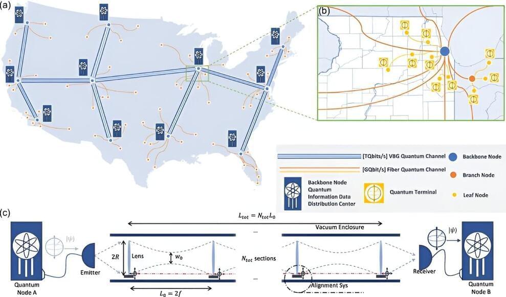
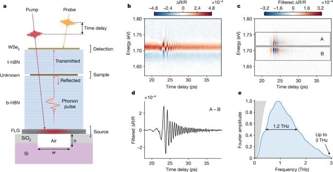
Toggle light / dark theme

The last time you dropped a favorite mug or sat on your glasses, you may have been too preoccupied to take much notice of the intricate pattern of cracks that appeared in the broken object. But capturing the formation of such patterns is the specialty of John Kolinski and his team at the Laboratory of Engineering Mechanics of Soft Interfaces (EMSI) in EPFL’s School of Engineering. They aim to understand how cracks propagate in brittle solids, which is essential for developing and testing safe and cost-effective composite materials for use in construction, sports, and aerospace engineering.

Southwest Research Institute has invested in research to enhance the capabilities of spacecraft instruments. Consequently, they have developed more effective conversion surfaces for the detection and analysis of low-energy particles in outer space.

Led by Dr. Jianliang Lin of Mechanical Engineering and Dr. Justyna Sokół of the Space Science Division, the project could potentially change our understanding of space physics and exploration.

Conventionally, corneal abrasion patients wear a clear, oxygen-permeable bandage contact lens for seven to 10 days but this treatment does not ensure the drug remains in the eye for sustained treatment, according to a statement by the University of Waterloo.

This new lens material was developed with the ambition to address the limitations of current methods for treating corneal abrasions. The contact lens material is derived from gelatin methacrylate, a collagen by-product. Collagen is a protein naturally found in the eye and is involved in the wound-healing process but it’s too soft and weak to perform as an appropriate contact lens material.

Dr. Evelyn Yim, an associate professor of chemical engineering at the University of Waterloo, found a way to transform gelatin methacrylate into a biomaterial ten times stronger than collagen, the statement revealed.

To enhance this efficiency, there is a requirement to fabricate electrodes with a . Unfortunately, existing technologies face challenges in achieving a uniform coating of ceramic materials within electrodes possessing intricate porous structures.

A collaborative research team, comprising Professor Jihwan An and Ph.D. candidate Sung Eun Jo from the Department of Mechanical Engineering at Pohang University of Science and Technology (POSTECH), and others, has successfully produced porous electrodes for SOFCs using latest semiconductor processes. This research has been featured as a back cover article in Small Methods.

The process of atomic layer deposition (ALD) involves depositing gaseous materials onto a substrate surface in thin, uniform atomic layers. In a recent study, Professor Jihwan An’s team, known for their prior work in enhancing the efficiency of SOFCs using ALD, developed and applied a powder ALD process and equipment. This enabled them to precisely coat nano-thin films on fine powders.

A research team, led by Professor Joonki Suh in the Department of Materials Science and Engineering and the Graduate School of Semiconductor Materials and Devices Engineering at UNIST, has made a significant breakthrough in thin film deposition technology. By employing an innovative atomic layer deposition (ALD) process, Professor Seo successfully achieved regular arrangement of tellurium (Te) atoms at low temperatures as low as 50 degrees Celsius.

The ALD method is a cutting-edge thin film process that enables precise stacking of semiconductor materials at the atomic layer level on three-dimensional structures—even at low process temperatures. However, traditional application to next-generation semiconductors requires high processing temperatures above 250 degrees Celsius and additional heat treatment exceeding 450 degrees Celsius.

In this research, the UNIST team applied ALD to monoelemental van der Waals tellurium—a material under extensive investigation for its potential applications in and thermoelectric materials.

Leafhoppers, a common backyard insect, secrete and coat themselves in tiny mysterious particles that could provide both the inspiration and the instructions for next-generation technology, according to a new study led by Penn State researchers. In a first, the team precisely replicated the complex geometry of these particles, called brochosomes, and elucidated a better understanding of how they absorb both visible and ultraviolet light.

This could allow the development of bioinspired optical materials with possible applications ranging from invisible cloaking devices to coatings to more efficiently harvest solar energy, said Tak-Sing Wong, professor of mechanical engineering and biomedical engineering. Wong led the study, which was published today (March 18) in the Proceedings of the National Academy of Sciences of the United States of America (PNAS).

As transistors are made ever tinier to fit more computing power into a smaller footprint, they bump up against a big problem: quantum mechanics. Electrons get jumpy in small devices and leak out, which wastes energy while degrading performance. Now a team of researchers is showing that it doesn’t have to be that way. With careful engineering, it’s possible to turn electrons’ quantum behavior into an advantage.

A team of English, Canadian, and Italian researchers have developed a single-molecule transistor that harnesses quantum effects. At low temperatures, the single-molecule device shows a strong change in current with only a small change in gate voltage, nearing a physical limit known as the sub-threshhold swing. Getting near or beyond this limit will allow transistors to be switched with lower voltages, making them more efficient and generating less waste heat. The research team, including physicists at Queen Mary University of London, achieved this by taking advantage of how quantum interference alters the flow of current in single molecules.

“We’ve demonstrated, in principle, that you can use destructive quantum interference for something useful.” —Jan Mol, Queen Mary University of London.

And the g-forces???


Rockets being passé, China is working on using an electromagnetic railgun to launch crewed spacecraft the size of a Boeing 737, weighing 50 tonnes, into orbit. This remarkably ambitious project is even more ambitious than it seems at first glance.

Call it a railgun, a catapult, or a mass driver, the idea of replacing rockets with an electromagnetic accelerator is a very attractive option. Instead of lifting off on chemical rockets that have to carry fuel and fuel to lift the fuel and fuel to lift the fuel and the additional fuel, it makes more sense to keep as much of the launching system on the ground while leaving the vehicle as light as possible.

The principle behind such a space railgun is simple, but the details are surprisingly complex and the numbers involved very quickly become daunting. If China can carry off using such a system to launch a spaceplane as part of its Tengyun project that began in 2016, it would be one of history’s major engineering achievements.