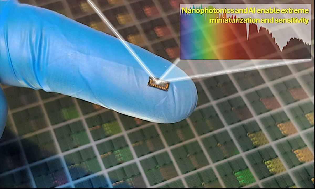
A new chip-scale spectrometer challenges the long-standing reliance on bulky optical systems by replacing physical light separation with computational reconstruction.
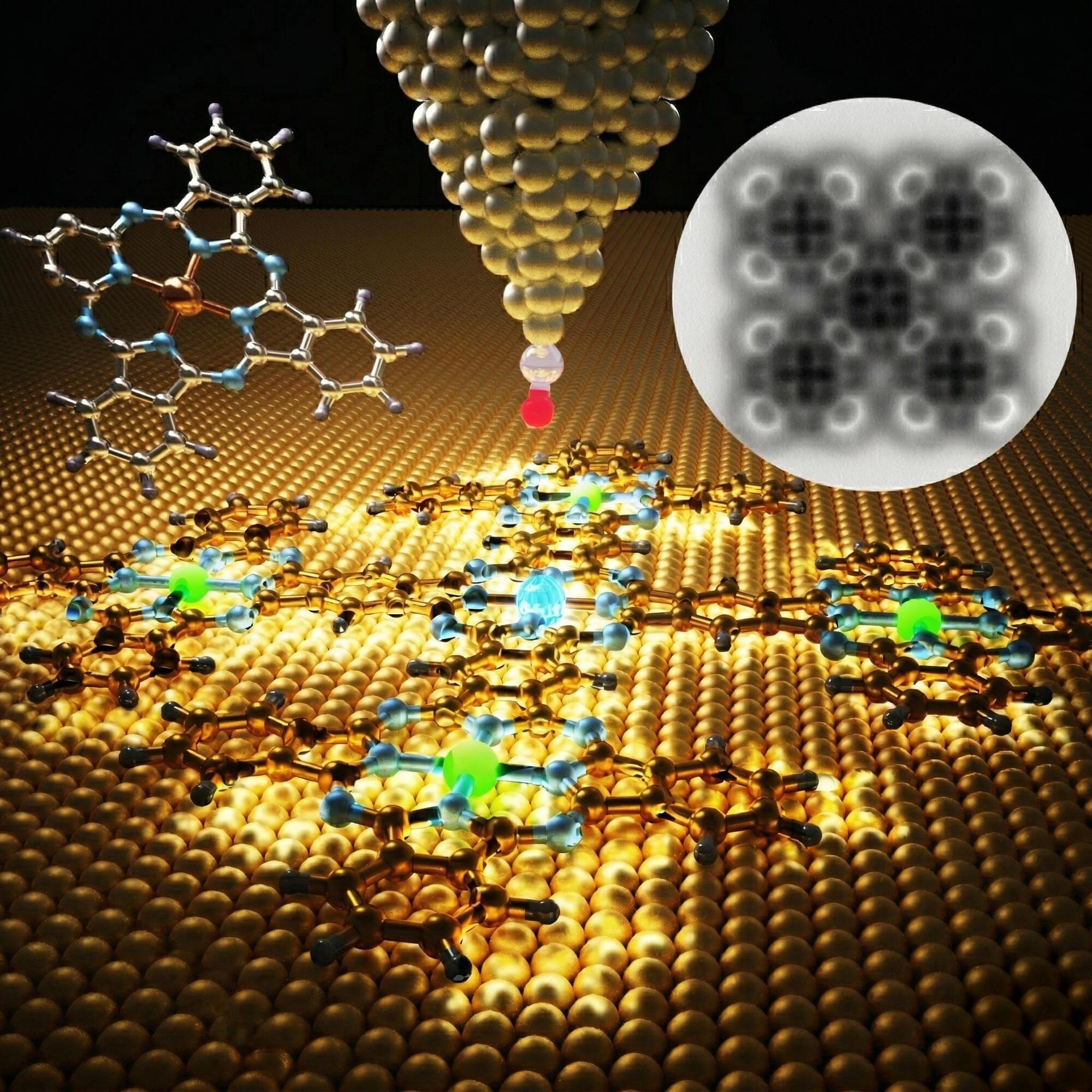
Scientists at the VIB–VUB Center for Structural Biology have uncovered a counterintuitive principle that could reshape how membrane proteins are designed from scratch: Sometimes, making a protein less stable helps it fold correctly. In their study published in the Proceedings of the National Academy of Sciences, the researchers demonstrate that introducing carefully placed “imperfections,” a strategy known as negative design, enables synthetic membrane proteins to fold and assemble efficiently in artificial membranes.
Membrane proteins are essential for life and biotechnology, acting as gateways, sensors, and drug targets. Yet designing them from scratch remains notoriously difficult. Unlike soluble proteins, they must navigate a complex folding process while inserting into lipid membranes and during this step, many designs fail.
Traditional protein design focuses on maximizing the stability of the final folded structure. But the new study shows that, for transmembrane β-barrel proteins, this approach can backfire.

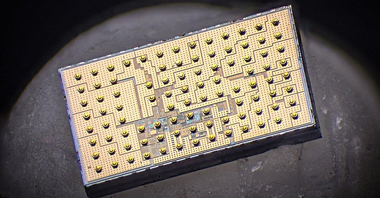
In an effort to meet the rising energy demands of data centers, engineers at the University of California San Diego have developed a new chip design that could improve how graphics processing units (GPUs) convert and manage power. The technology demonstrates a more efficient way to perform a critical task in electronics: converting high voltages into lower levels required by computing hardware. In lab tests, a prototype chip performed the type of voltage conversion used in modern data centers with high efficiency.
The advance, published in Nature Communications, could lead to the development of smaller, more energy-efficient systems for advanced computing.
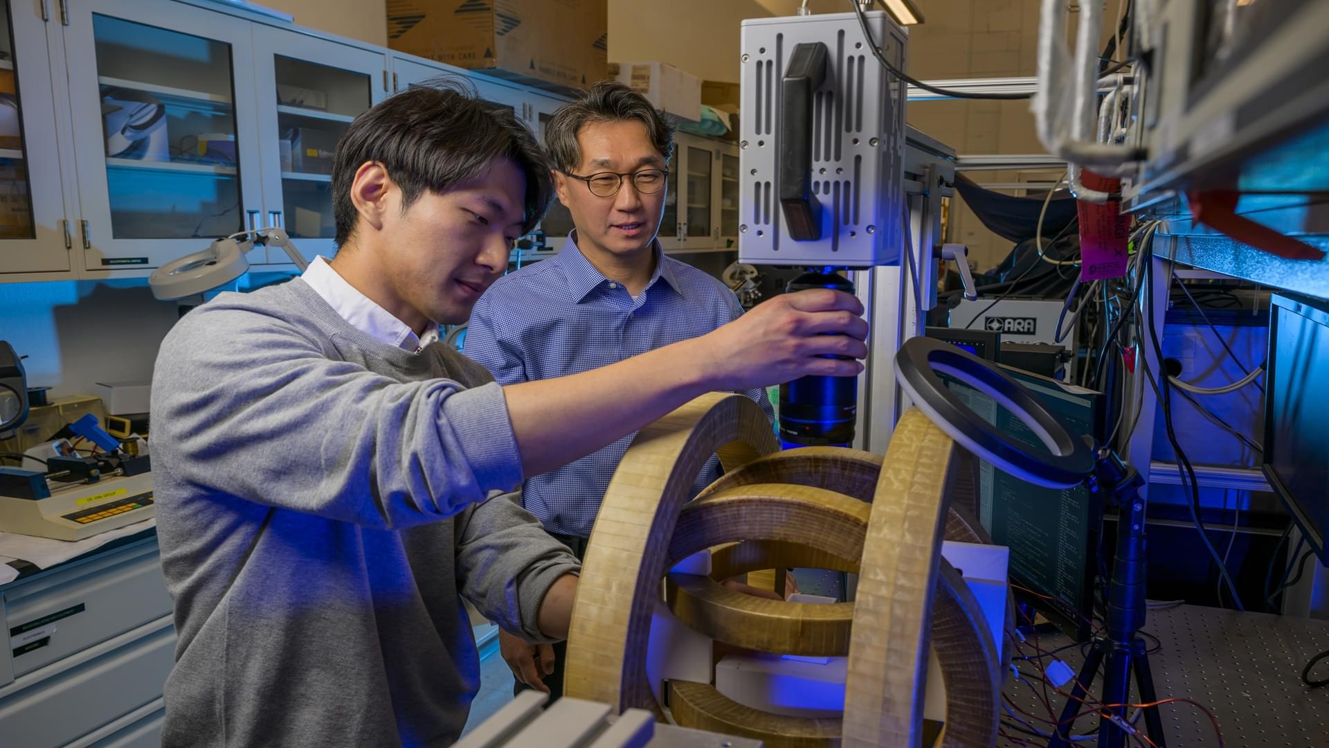
Electrons have three intrinsic properties: spin, charge and orbital angular momentum. Researchers have long studied how to use spin to more efficiently create an electrical current. But the field of orbitronics—which is based upon using an electron’s orbital angular momentum, rather than its spin, to create a current flow—remains relatively new.
“Traditionally, it has been technically challenging to generate orbital current,” says Dali Sun, a professor of physics and member of the Organic and Carbon Electronics Lab (ORaCEL) at NC State University.
In a recent study, however, Sun and an international team of researchers demonstrated a groundbreaking new method to generate orbital current.

