Distributed fiber-optic sensors are widely used to monitor temperature and strain in infrastructure, but their spatial resolution has long been limited. In a new study, researchers from Shibaura Institute of Technology and Yokohama National University, Japan, have demonstrated that operating near a previously avoided frequency regime and suppressing signal distortions allows reflection-based sensing to achieve a world-record spatial resolution of 6 mm among single-end-access configurations. This enables precise monitoring of temperature and strain in infrastructure.
Distributed fiber-optic sensing technologies play a crucial role in monitoring temperature and strain across large structures such as bridges, tunnels, pipelines, and buildings. Unlike conventional point sensors, distributed fiber-optic sensors provide continuous measurements along their entire length, allowing early detection of damage or abnormal conditions. However, one persistent challenge has been spatial resolution—the ability to pinpoint exactly where a change occurs. Improving resolution without complicating system design has remained a central goal in fiber-optic sensing research.
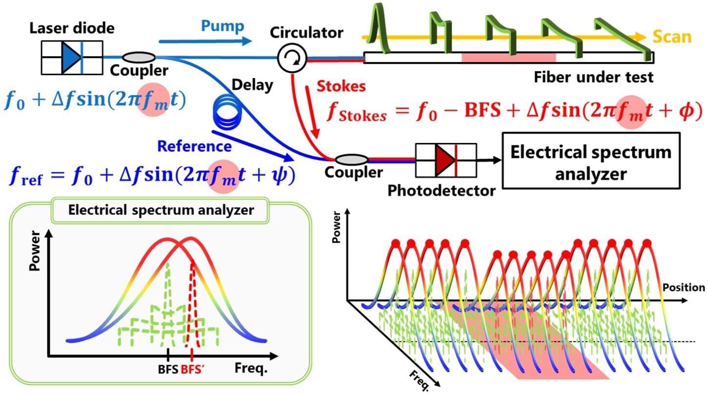
One promising technique, known as Brillouin optical correlation-domain reflectometry (BOCDR), enables distributed sensing using light injected from only one end of the fiber. This reflection-based configuration simplifies installation and allows measurements even if the fiber is damaged. BOCDR also offers higher spatial resolution than many other Brillouin-based methods. Yet, its performance has been constrained by a widely accepted assumption: operating near or beyond the Brillouin bandwidth, a frequency range intrinsic to the fiber, was believed to cause unstable signals and unreliable measurements. As a result, this operating regime has largely been avoided, limiting achievable resolution.


