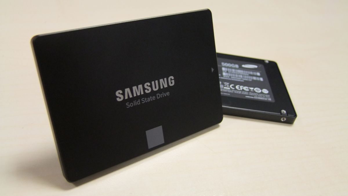
Intel unveiled its new Optane line of SSDs at IDF this week, with a focus on high performance and endurance. The drives should be shipping to the consumer market in 2016.
Category: electronics – Page 108
A new optical chip that can process photons in a dizzying number of infinite ways has been developed by two research teams. Researchers from the University of Bristol in the UK and Nippon Telegraph and Telephone in Japan (NTT) are behind the breakthrough in quantum computing. The means to solve daunting problems such as the ability to design new life-saving drugs; perform advanced calculations that are a step or two beyond even supercomputers; and analyze weather patterns for more accurate forecasting has just received a major boost.
A group of researchers have pulled off a staggering feat; they’ve developed a silicon-based optical chip that is fully reprogrammable and can process photons in every way imaginable and then some, reports Phys.org.
Prof. Jeremy O’Brien, the Director of the Centre for Quantum Photonics at Bristol University where researchers masterminded the development of the chip, said:
Researchers from the University of Bristol in the UK and Nippon Telegraph and Telephone (NTT) in Japan, have developing an optical chip that can process photons in an infinite number of ways.
It’s a major step forward in creating a quantum computer to solve problems such as designing new drugs, superfast database searches, and performing otherwise intractable mathematics that aren’t possible for super computers.
The fully reprogrammable chip brings together a multitude of existing quantum experiments and can realise a plethora of future protocols that have not even been conceived yet, marking a new era of research for quantum scientists and engineers at the cutting edge of quantum technologies.
The microprocessor inside a computer is a single multipurpose chip that has revolutionised people’s life, allowing them to use one machine to surf the web, check emails and keep track of finances.
Now, researchers from the University of Bristol in the UK and Nippon Telegraph and Telephone (NTT) in Japan, have pulled off the same feat for light in the quantum world by developing an optical chip that can process photons in an infinite number of ways.
Gone are the days when you have to sacrifice size for speed with an SSD drive in your laptop. At the Flash Memory Summit in California, Samsung just revealed a new 2.5-inch SSD drive with an incredible 16 terabytes of storage. It’s not only the world’s largest SSD—it’s actually now the world’s largest hard drive, period.
So how on Earth did Samsung pull off a such an incredible feat? Inside the PM1633a SSD you’ll find stacks and stacks of the company’s latest and greatest 256Gbit NAND flash dies, which are twice the capacity of the 128Gbit NAND flash dies currently in use. According to Ars Technica’s calculations, there should be somewhere around 480 to 500 of the dies inside Samsung’s new SSD. Which is even more impressive given it still fits inside a 2.5-inch housing, although it’s probably a lot taller than most.
The answer to the million dollar question about the new 16TB SSD—how much does it cost?—is thankfully not a million dollars. However, the first units will probably sell in the range of $5,000 to $7,000 and will be targeted for use in servers and other enterprise applications. But over time, as with all technology, the massive SSDs will certainly drop in price and trickle down to consumers—just in time for our storage demands spiking thanks to 4K movie downloads.
The Defense Advanced Research Projects Agency (DARPA) website reports that two of DARPA’s Young Faculty Award (YFA) recipients have developed nanoscale electronic switches with reprogrammable features, similar to those at play in inter-neuron communication in the brain, which could find uses in next-generation reconfigurable electronic devices and brain-inspired computing.
Intel and Micron Technology on Tuesday unveiled what they touted as a new kind of memory chip that could “revolutionize” computing devices, services and applications.
Intel and Micron have a new way to store data that they say is denser, tougher, and faster than the competition, and it’s already starting production. In a live keynote today, the companies announced 3D Xpoint, a new category of non-volatile memory that claims to be 1,000 times faster than the NAND architecture underlying most flash memory cards and solid state drives. The new architecture does without transistors entirely, relying on a bulk material property change to switch bits from a low-resistance to a high-resistance state. From there, memory cells are layered in an intricate three-dimensional checkerboard pattern that Intel researchers say is 10 times denser than conventional memory.
UT Dallas scientists have constructed novel fibers by wrapping sheets of tiny carbon nanotubes to form a sheath around a long rubber core. This illustration shows complex two-dimensional buckling, shown in yellow, of the carbon nanotube sheath/rubber-core fiber. The buckling results in a conductive fiber with super elasticity and novel electronic properties. (credit: UT Dallas Alan G. MacDiarmid Nanotech Institute)
An international research team based at The University of Texas at Dallas has made electrically conducting fibers that can be reversibly stretched to more than 14 times their initial length and whose electrical conductivity increases 200-fold when stretched.
UC Berkeley engineers, in collaboration with colleagues at Taiwan’s National Chiao Tung University, have developed a 3D printing process for creating basic electronic components, such as resistors, inductors, capacitors, and integrated wireless electrical sensing systems.