Quantum solutions may be obtained from beautiful pictures of interfering BECs.

Industrial powerhouse Honeywell says its latest quantum computer is now the fastest in the world. How quickly real-world applications will develop or how swiftly they’ll be able to impact industries or affect cryptographic systems such as Bitcoin is the subject of rigorous debate.
In an announcement on Thursday, Honeywell says its team of scientists, engineers and technicians has delivered a quantum volume of 64. The metric measures both the total number of the computer’s qubits and how well it handles them. IBM’s machine scored a 32, suggesting Honeywell’s quantum computer is twice as fast.
Honeywell’s machine is designed to add up to 640,000 quantum bits (qubits) as the system scales. Tony Uttley, president of Honeywell’s quantum computing division, tells CNET.
Honeywell stock doesn’t trade on quantum fundamentals yet. Shares are down about 16% year to date, worse than the comparable drops of the S&P 500 and Dow Jones Industrial Average. Honeywell is a large aerospace supplier, and the commercial aviation business has been hammered by Covid-19. Boeing (BA) stock, for instance, is off more than 40% year to date.
Honeywell stock is flat in early Friday trading. The S&P is up about 0.8%.
The quantum-computing industry hasn’t yet arrived, despite today’s announcement. But quantum computers are already better than regular computers in certain instances. Google parent Alphabet (GOOGL) demonstrated the ability of its rudimentary quantum computer to beat traditional systems.

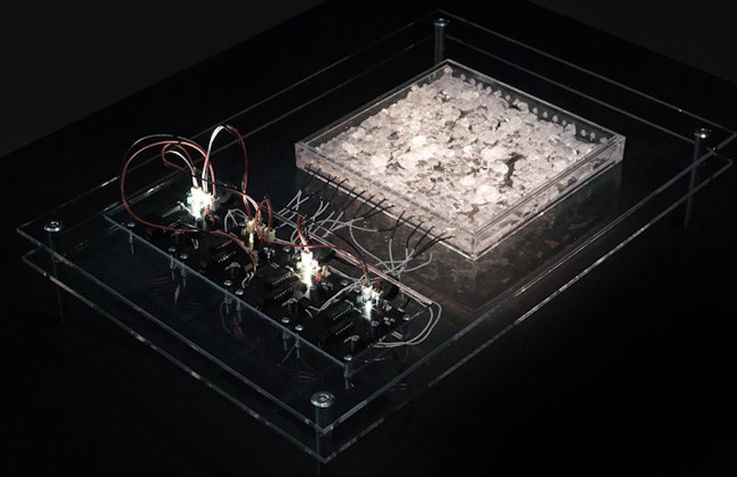
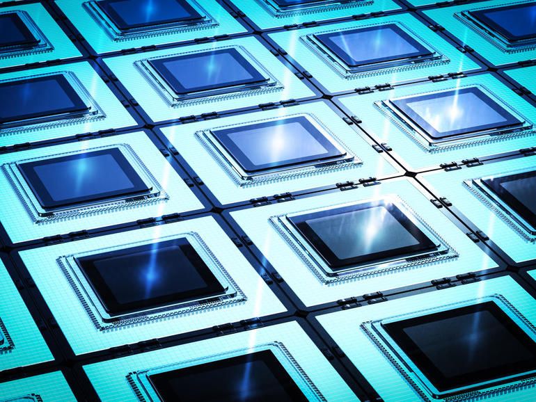
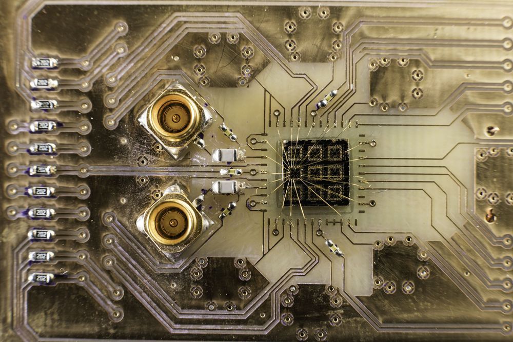
Computers are renowned for flexibility, running everything from game consoles to stock exchanges. But at the level of computation, most computers rely on arrays of identical processors called cores. Now, a team at Princeton University has built a hardware platform that allows different kinds of computer cores to fit together, allowing designers to customize systems in new ways.
The goal is to create new systems that parcel out tasks among specialized cores, increasing efficiency and speed.
On top of multi–core collaboration, even more gains are achievable when cores needn’t all rely on the same basic programming code that tells a core how to handle its processing jobs. Designers call this basic code an Instruction Set Architecture (ISA). Well-established ISAs include Intel x86, commonly found in laptops, ARM in smartphones, and POWER in IBM mainframes. Besides mixing together cores specialized for different ISAs, researchers are also interested in developing hybrid ISAs to underpin new processor designs, exploiting the potential of new, cutting-edge, open-source ISAs like RISC-V ISA.
“Beam me up” is one of the most famous catchphrases from the Star Trek series. It is the command issued when a character wishes to teleport from a remote location back to the Starship Enterprise.
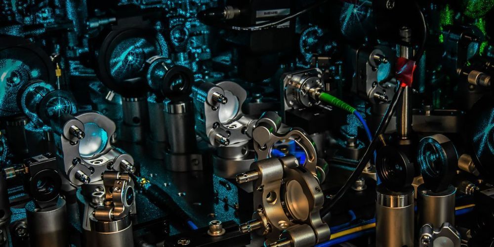
While human teleportation exists only in science fiction, teleportation is possible in the subatomic world of quantum mechanics—albeit not in the way typically depicted on TV. In the quantum world, teleportation involves the transportation of information, rather than the transportation of matter.
Last year scientists confirmed that information could be passed between photons on computer chips even when the photons were not physically linked.