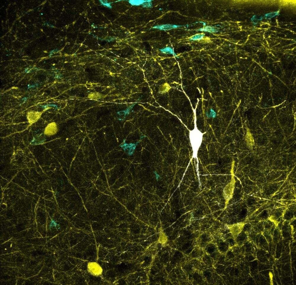
A study led by researchers from the Institute Cajal of Spanish Research Council (CSIC) in Madrid, Spain in collaboration with the Bioengineering Department of George Mason University in Virginia, U.S. has updated one of the world’s largest databases on neuronal types, Hippocampome.org.
The study, which is published in the journal PLOS Biology, represents the most comprehensive mapping performed to date between neural activity recoded in vivo and identified neuron types. This major breakthrough may enable biologically meaningful computer modeling of the full neuronal circuit of the hippocampus, a region of the brain involved in memory function.
Circuits of the mammalian cerebral cortex are made up of two types of neurons: Excitatory neurons, which release a neurotransmitter called glutamate, and inhibitory neurons, which release GABA (gamma-aminobutanoic acid), the main inhibitor of the central nervous system. “A balanced dialogue between the ‘excitatory’ and ‘inhibitory’ activities is critical for brain function. Identifying the contribution from the several types of excitatory and inhibitory cells is essential to better understand brain operation,” explains Liset Menendez de la Prida, the Director of the Laboratorio de Circuitos Neuronales at the Institute Cajal who leads the study at the CSIC.
Asia’s top chip stocks tumbled Tuesday, ensnared in an escalating US-China tech race that has erased more than $240 billion from the sector’s global market value.
Taiwan Semiconductor Manufacturing Co., the world’s largest contract chipmaker, plunged a record 8.3% while Samsung Electronics Co. and Tokyo Electron Ltd. also declined. The selloff spread to the foreign-exchange market as investors tallied up the damage from the sweeping curbs the US is imposing on companies that conduct technology business with China.
In this episode we explore a User Interface Theory of reality. Since the invention of the computer virtual reality theories have been gaining in popularity, often to explain some difficulties around the hard problem of consciousness (See Episode #1 with Sue Blackmore to get a full analysis of the problem of how subjective experiences might emerge out of our brain neurology); but also to explain other non-local anomalies coming out of physics and psychology, like ‘quantum entanglement’ or ‘out of body experiences’. Do check the devoted episodes #4 and #28 respectively on those two phenomena for a full breakdown. As you will hear today the vast majority of cognitive scientists believe consciousness is an emergent phenomena from matter, and that virtual reality theories are science fiction or ‘Woowoo’ and new age. One of this podcasts jobs is to look at some of these Woowoo claims and separate the wheat from the chaff, so the open minded among us can find the threshold beyond which evidence based thinking, no matter how contrary to the consensus can be considered and separated from wishful thinking. So you can imagine my joy when a hugely respected cognitive scientist and User Interface theorist, who can cut through the polemic and orthodoxy with calm, respectful, evidence based argumentation, agreed to come on the show, the one and only Donald D Hoffman.
Hoffman is a full professor of cognitive science at the University of California, Irvine, where he studies consciousness, visual perception and evolutionary psychology using mathematical models and psychophysical experiments. His research subjects include facial attractiveness, the recognition of shape, the perception of motion and colour, the evolution of perception, and the mind-body problem. So he is perfectly placed to comment on how we interpret reality.
Hoffman has received a Distinguished Scientific Award of the American Psychological Association for early career research into visual perception, the Rustum Roy Award of the Chopra Foundation, and the Troland Research Award of the US National Academy of Sciences. So his recognition in the field is clear.
He is also the author of ‘The Case Against Reality’, the content of which we’ll be focusing on today; ‘Visual Intelligence’, and the co-author with Bruce Bennett and Chetan Prakash of ‘Observer Mechanics’.
What we discuss: 00:00 Intro. 05:30 Belief VS questioning. 11:20 Seeing the world for survival VS for knowing reality as it truly is. 13:30 Competing strategies to maximise ‘fitness’ in the evolutionary sense. 15:22 Fitness payoff’s can be calculated as mathematical functions, based on different organisms, states and actions. 17:00 Evolutionary Game Theory computer simulations at UC Irvine. 21:30 The payoff functions that govern evolution do not contain information about the structure of the world. 25:00 The world is NOT as it seems VS The world is NOTHING like it seems. 29:30 Space-time cannot be fundamental. 32:30 Local and non-contextual realism have been proved false. 37:45 A User-Interface network of conscious agents. 41:30 A virtual reality computer analogy. 43:30 Space and time and physical objects are merely a user interface. 49:30 Reductionism is false. 53:30 User Interface theory VS Simulation theory. 56:30 Panpsychists are fundamentally physicalists. 57:30 Making mathematical predictions about conscious agents. 59:30 Like space and time maths are invented metrics, so must we start with consciousness metrics. 01:03:30 Experiences lead to actions, which affect other agent’s conscious experiences. 01:08:00 The notion of truth is deeper than the notion of proof and theory. 01:10:00 Consciousness projects space-time so it can explore infinite possibilities. 01:13:00 ‘Not that which the eye can see, but that whereby the eye can see’, Kena Upanishad. 01:17:30 Is nature written in the language of Maths? 01:27:00 Consciousness is like the living being, and maths is like the bones. 01:34:50 Don Hoffman on Max Tegmark’s ‘Everything that is mathematically possible is real’ 01:48:00 Different analogies for different eras.
Francis Heylighen started his career as yet another physicist with a craving to understand the foundations of the universe – the physical and philosophical laws that make everything tick. But his quest for understanding has led him far beyond the traditional limits of the discipline of physics. Currently he leads the Evolution, Complexity and COgnition group (ECCO) at the Free University of Brussels, a position involving fundamental cybernetics research cutting across almost every discipline. Among the many deep ideas he has pursued in the last few decades, one of the most tantalizing is that of the Global Brain – the notion that the social, computational and communicative matrix increasingly enveloping us as technology develops, may possess a kind of coherent intelligence in itself.
I first became aware of Francis and his work in the mid-1990s via the Principia Cybernetica project – an initiative to pursue the application of cybernetic theory to modern computer systems. Principia Cybernetica began in 1989, as a collaboration between Heylighen, Cliff Joslyn, and the late great Russian physicist, dissident and systems theorist Valentin Turchin. And then 1993, very shortly after Tim Berners-Lee released the HTML/HTTP software framework and thus created the Web, the Principia Cybernetica website went online. For a while after its 1993 launch, Principia Cybernetica was among the largest and most popular sites on the Web. Today the Web is a different kind of place, but Principia Cybernetica remains a unique and popular resource for those seeking deep, radical thinking about the future of technology, mind and society.
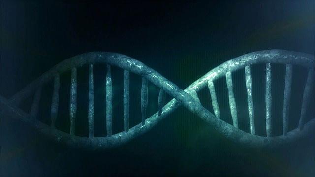
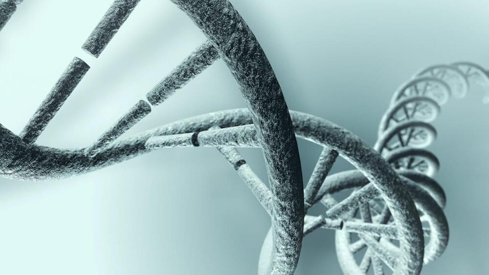
Amid much speculation and research about how our genetics affect the way we age, a University of California, Berkeley, study now shows that individual differences in our DNA matter less as we get older and become prone to diseases of aging, such as diabetes and cancer.
In a study of the relative effects of genetics, aging and the environment on how some 20,000 human genes are expressed, the researchers found that aging and environment are far more important than genetic variation in affecting the expression profiles of many of our genes as we get older. The level at which genes are expressed — that is, ratcheted up or down in activity — determines everything from our hormone levels and metabolism to the mobilization of enzymes that repair the body.
“How do your genetics — what you got from your sperm donor and your egg donor and your evolutionary history — influence who you are, your phenotype, such as your height, your weight, whether or not you have heart disease?” said Peter Sudmant, UC Berkeley assistant professor of integrative biology and a member of the campus’s Center for Computational Biology. “There’s been a huge amount of work done in human genetics to understand how genes are turned on and off by human genetic variation. Our project came about by asking, ‘How is that influenced by an individual’s age?’ And the first result we found was that your genetics actually matter less the older you get.”
🙏 We would like to thank our generous Patreon supporters who make Two Minute Papers possible: Aleksandr Mashrabov, Alex Balfanz, Alex Haro, Andrew Melnychuk, Benji Rabhan, Bryan Learn, B Shang, Christian Ahlin, Eric Martel, Geronimo Moralez, Gordon Child, Jace O’Brien, Jack Lukic, John Le, Jonas, Jonathan, Kenneth Davis, Klaus Busse, Kyle Davis, Lorin Atzberger, Lukas Biewald, Luke Dominique Warner, Matthew Allen Fisher, Michael Albrecht, Michael Tedder, Nevin Spoljaric, Nikhil Velpanur, Owen Campbell-Moore, Owen Skarpness, Rajarshi Nigam, Ramsey Elbasheer, Steef, Taras Bobrovytsky, Ted Johnson, Thomas Krcmar, Timothy Sum Hon Mun, Torsten Reil, Tybie Fitzhugh, Ueli Gallizzi. If you wish to appear here or pick up other perks, click here: https://www.patreon.com/TwoMinutePapers.
From driving water wheels to turning turbines, waterhas been used as the prime mover of machinery and the powerhouse of industry for many centuries. In ancient times, the forces of flowing water were even harnessed to power the first rudimentaryclocks. Now, engineers at Stanford University have created the world’s first water-operated computer. Using magnetized particles flowing through a micro-miniature network ofchannels, the machine runs like clockwork and is claimed to be capable ofperforming complex logical operations.
Using poppy-seed sizeddroplets of water impregnated with magnetic nanoparticles (those handy little elementsbeing used in everything from drug delivery inhumans to creating e-paper whiteboards), the new fluidic computer uses electromagnetic fields to accurately pump thesedroplets around a set of physical gates to perform logical operations. Suspendedin oil and timed to move in very specific steps, the droplets in the system cantheoretically be used to accomplish any process that a normal electroniccomputer can, albeit at considerably slower speeds.
Stanford assistant professor Manu Prakash has spent almost a decadethinking about such a device, ever since he was a graduate student. The manyand varied components required of a fluidic computer have slowly coalesced inhis mind over that time, with the most fundamental component of all – an accurateoperating clock to drive the logic – being the crucial element in bringing hisinvention to fruition. Ultimately, Prakash built a rotating magnetic field to synchronize the flow of all the droplets in a precisely timed manner, andact as the clock.
A liquid hard drive containing a suspension of nanoparticles could be used to store impressive amounts of data: 1 terabyte per tablespoon.
Researchers from the University of Michigan and New York University have been simulating wet information storage techniques which uses clusters of nanoparticles suspended in liquid. These clusters of particles can store more data than conventional computer bits which have just two storage states: 0 and 1. The clusters of particles work a bit like Rubik’s Cubes to reconfigure in different ways to represent different storage states. A 12-particle memory cluster connected to a central sphere can have almost eight million unique states, which is equivalent to 2.86 bytes of data.
The system works by having nanoparticles attached to a central sphere. When the sphere is small, the outer particles trap each other into place, storing data. If the sphere is a bit larger, the particles can be reconfigured to store different information. The team created a cluster involving four particles on a central sphere — all made of polymers. By heating the liquid up, the spheres expand and the particles can rearrange themselves in predictable ways. Although the four-particle clusters have only two distinguishable configurations (i.e. like a regular bit), the plan is create clusters with many more particles.
A new study challenges the common belief that human brain’s functions such as learning, memory, and perception occur in the central part of neurons called soma. In a brain structure, neurons’ three-like feature has soma in the middle and branches called dendrites. Soma will spike whenever there is data that needs processing and dendrites will communicate with each other — but not until the University of California, Los Angeles discovered the opposite.
UCLA team tested the theory of “soma to dendrites” and found a contradicting result. Dendrites are electrically active and generate 10 times more spikes that somas. Scientists are now on to new finding that dendrites’ role is to form and store memories.
According to Mayank Mehta, senior author of the study, dendrites are not passive conduits. They themselves are moving around freely and generate spikes or brain activity. This also shows that 90 percent of the brain is being utilized since dendrites comprise 90 percent of the brain tissue. Meaning, the human brain has almost 10 times more computational capability than previously thought.