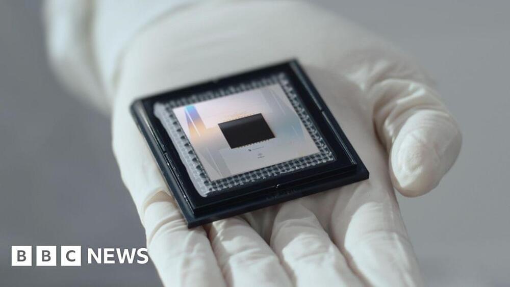
Toggle light / dark theme

Can We Build an Artificial Hippocampus?

To try everything Brilliant has to offer—free—for a full 30 days, visit http://brilliant.org/ArtemKirsanov/
The first 200 of you will get 20% off Brilliant’s annual premium subscription.

My name is Artem, I’m a computational neuroscience student and researcher. In this video we discuss the Tolman-Eichenbaum Machine – a computational model of a hippocampal formation, which unifies memory and spatial navigation under a common framework.

Patreon: https://www.patreon.com/artemkirsanov.
Twitter: https://twitter.com/ArtemKRSV

OUTLINE:
00:00 — Introduction.
01:13 — Motivation: Agents, Rewards and Actions.
03:17 — Prediction Problem.
05:58 — Model architecture.
06:46 — Position module.
07:40 — Memory module.
08:57 — Running TEM step-by-step.
11:37 — Model performance.
13:33 — Cellular representations.
17:48 — TEM predicts remapping laws.
19:37 — Recap and Acknowledgments.
20:53 — TEM as a Transformer network.
21:55 — Brilliant.
23:19 — Outro.

REFERENCES:
1. Whittington, J. C. R. et al. The Tolman-Eichenbaum Machine: Unifying Space and Relational Memory through Generalization in the Hippocampal Formation. Cell 183, 1249–1263.e23 (2020).
2. Whittington, J. C. R., Warren, J. & Behrens, T. E. J. Relating transformers to models and neural representations of the hippocampal formation. Preprint at http://arxiv.org/abs/2112.04035 (2022).
3. Whittington, J. C. R., McCaffary, D., Bakermans, J. J. W. & Behrens, T. E. J. How to build a cognitive map. Nat Neurosci 25, 1257–1272 (2022).

CREDITS:

Simulating the Cosmos: Is a Miniature Universe Possible?

Wouldn’t it be nice to have a computer answer all of the biggest questions in the universe?

In his first year of graduate school, in 2013, Michael Wagman walked into his advisor’s office and asked, “Can you help me simulate the universe?”

Wagman, a theoretical physicist and associate scientist at the US Department of Energy’s Fermi National Accelerator Laboratory, thought it seemed like a reasonable question to ask. “We have all of these beautiful theoretical descriptions of how we think the world works, so I wanted to try and connect those formal laws of physics to my everyday experience of reality,” he says.

Will quantum cryptography soon be essential for IoT security?

As connectivity continues to expand and the number of devices on a network with it, IoT’s ambition of creating a world of connected things grows. Yet, with pros, comes the cons, and the flip side of this is the growing security challenges that come with it too.

Security has been a perennial concern for IoT since it’s utilisation beyond its use for basic functions like tallying the stock levels of a soda machine. However, for something of such interest to the industry, plans for standardisation remain allusive. Instead, piece meal plans to ensure different elements of security, like zero trust for identity and access management for devices on a network, or network segmentation for containing breaches, are undertaken by different companies according to their needs.

Yet with the advancement of technology, things like quantum computing pose a risk to classic cryptography methods which, among other things, ensures data privacy is secure when being transferred from device to device or even to the Cloud.

Integrated Circuits based on a 2D Semiconductor Operating at GHz Frequencies

Transistors are crucial electronic components that regulate, amplify and control the flow of current inside most existing devices. In recent years, electronics engineers have been trying to identify materials and design strategies that could help to further improve the performance of transistors, while also reducing their size.

Two-dimensional (2D) transition metal dichalcogenides have some advantageous properties that could help to enhance the capabilities of transistors. While past studies have demonstrated the potential of these materials in individual transistors, their use for developing entire integrated circuits (ICs) that operate at high frequencies has proved challenging.

Researchers at Nanjing University in China recently created new ICs that can operate at GHz frequencies, based on the 2D semiconducting material monolayer molybdenum disulfide (MoS2). Their devices, presented in a Nature Electronics paper, rely on MoS2-based field-effect transistors (FETs).

What Is Quantum Advantage? A Quantum Computing Scientist Explains An Approaching Milestone Marking The Arrival Of Extremely Powerful Computers

Quantum advantage is the milestone the field of quantum computing is fervently working toward, where a quantum computer can solve problems that are beyond the reach of the most powerful non-quantum, or classical, computers.

Quantum refers to the scale of atoms and molecules where the laws of physics as we experience them break down and a different, counterintuitive set of laws apply. Quantum computers take advantage of these strange behaviors to solve problems.

There are some types of problems that are impractical for classical computers to solve, such as cracking state-of-the-art encryption algorithms. Research in recent decades has shown that quantum computers have the potential to solve some of these problems. If a quantum computer can be built that actually does solve one of these problems, it will have demonstrated quantum advantage.

DARPA and Materials

In 1960, DARPA funded three university-based Inderdisciplinary Laboratories (IDLs) that opened the way toward an enormous field of research and development known today as materials science and engineering. In this video, DARPA program managers, DARPA-funded researchers, and a Naval Research Laboratory scientist tell this field-building story as it unfolded over the past six decades, all the while delivering breakthroughs in the way materials are designed, processed, and deployed to push technologies forward. Intelligent processing of materials (IPM), accelerated insertion of materials (AIM), and integrated computational materials engineering (ICME) are among the specific programs detailed in the video. DARPA is currently developing technologies that enable the crafting of new materials with unprecedented properties by designing and controlling matter from atoms on up to human-scale systems.

NSF awards team $2M to develop faster and more efficient semiconductors

The COVID-19 pandemic supply shortfalls and geopolitical issues cast a bright light on the decline of semiconductor manufacturing in the United States, down from 37 percent of the global total in 1993 to about 12 percent now. The Creating Helpful Incentives to Produce Semiconductors and Science Act of 2022 (CHIPS Act) directed $280 billion in spending, with the bulk on scientific research and development.

America needs better computer chips.

Mobile devices are ubiquitous; we carry them around in a pocket or purse and use them for everyday tasks. However, they are connected to centralized servers and thus cannot learn much about or adjust to their complicated and changing environments independently.

Midcircuit Operations in Atomic Arrays

Three research groups have exploited the nuclear spins of ytterbium-171 to manipulate qubits before they are read out—an approach that could lead to efficient error-correction schemes for trapped-atom computing platforms.

Quantum computing on neutral-atom platforms has reached remarkable milestones in the past two decades. However, researchers have yet to overcome a key barrier to the realization of a neutral-atom-based quantum computer: the efficient correction of errors. In principle that barrier can be lowered with so-called midcircuit operations. These operations involve probing the quantum state of “ancilla” qubits without disturbing nearby “data” qubits used for computation. The ancilla qubit measurements can indicate whether the data qubits have undergone faulty operations, allowing for the data qubits to be corrected midcircuit—that is, during the execution of the computation rather than after its completion. Now three independent research groups have achieved midcircuit operation, or made progress toward this goal, with a novel choice of atom: ytterbium-171 (171 Yb) [13].

A neutral-atom qubit platform consists of a two-dimensional (2D) array of atoms trapped by optical tweezers—tightly focused laser beams whose wavelengths are tuned far away from the atomic transitions. The size of the traps, limited by diffraction, is typically about 1 µm. Thanks to the large electric-dipole force from the focused laser and to a high vacuum, the atoms can stay trapped for as long as tens of seconds.

Windows Hello auth bypassed on Microsoft, Dell, Lenovo laptops

Security researchers bypassed Windows Hello fingerprint authentication on Dell Inspiron, Lenovo ThinkPad, and Microsoft Surface Pro X laptops in attacks exploiting security flaws found in the embedded fingerprint sensors.

Blackwing Intelligence security researchers discovered vulnerabilities during research sponsored by Microsoft’s Offensive Research and Security Engineering (MORSE) to assess the security of the top three embedded fingerprint sensors used for Windows Hello fingerprint authentication.

Blackwing’s Jesse D’Aguanno and Timo Teräs targeted embedded fingerprint sensors made by ELAN, Synaptics, and Goodix on Microsoft Surface Pro X, Lenovo ThinkPad T14, and Dell Inspiron 15.