A new study from Rice shows how to turn data center waste into power.


The neutral atom array architecture for quantum computing has been rapidly advancing over the last several years, and a recent study published in Nature has just revealed another step forward for this technology. The team of Harvard researchers involved in this study have engineered a 3,000-qubit neutral atom array system capable of operating continuously for more than two hours, which goes far beyond typical trap lifetimes of only about 60 seconds.
Typically, neutral atom array systems arrange neutral atoms, like rubidium, in an array using highly focused laser beams, called optical tweezers. The individual atoms are arranged and held under vacuum conditions and then used as qubits to perform quantum computing and other operations. However, the procedure results in the loss of some atoms.
“An outstanding challenge associated with these systems involves atom loss, originating from errors in entangling operations, state-readout, and finite trap lifetime. Atom losses necessitate pulsed operation which limits the performance of these quantum systems, including the circuit depth of quantum computation, accuracy of atomic clocks, and the rate of entanglement generation in quantum networking protocols,” the study authors explain.
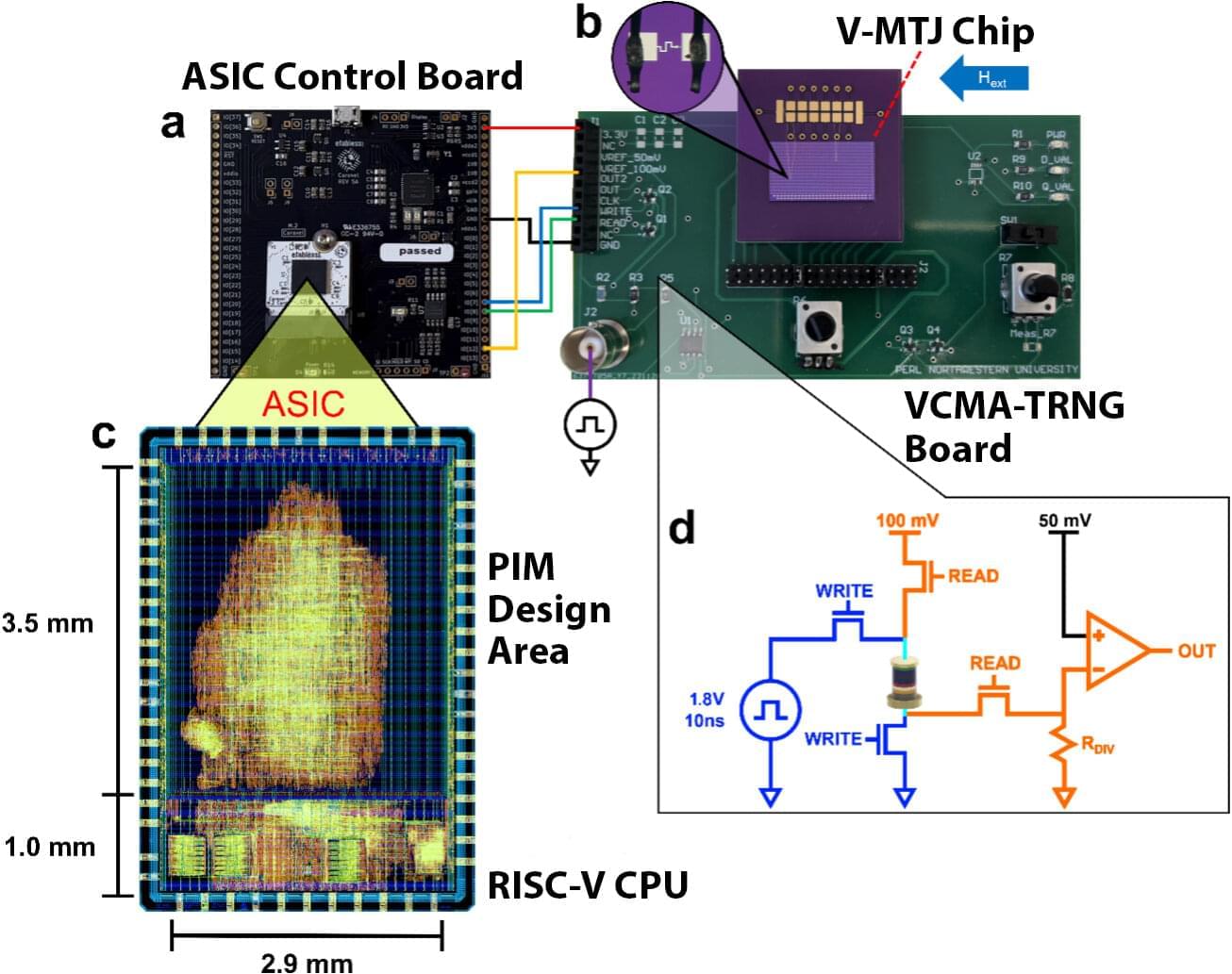
Probabilistic Ising machines (PIMs) are advanced and specialized computing systems that could tackle computationally hard problems, such as optimization or integer factorization tasks, more efficiently than classical systems. To solve problems, PIMs rely on interacting probabilistic bits (p-bits), networks of interacting units of digital information with values that randomly fluctuate between 0 and 1, but that can be biased to converge to yield desired solutions.

Interesting paper where microintravascular electrodes were inserted into cortical veins of pigs to record somatosensory and visual neuronal activity as well as selectively stimulate motor areas. Compared to electrocorticography, this is a less invasive approach with similar capabilities. #neurotech [ https://doi.org/10.1002/aisy.202500487](https://doi.org/10.1002/aisy.202500487)
Intravascular electroencephalography (ivEEG) with microintravascular electrodes enhances neural monitoring, functional mapping, and brain–computer interfaces (BCIs), offering a minimally invasive approach to assess cortical activities; however, this approach remains unrealized. Current ivEEG methods using electrode-attached stents are limited to recording from large vessels, such as the superior sagittal sinus (SSS), restricting access to cortical regions essential for precise BCI control, such as those for hand and mouth movements. Here, ivEEG signals from small and soft cortical veins (CV-ivEEGs) in eight pigs using microintravascular electrodes are recorded, achieving higher resting-state signal power and greater spatial resolution of somatosensory evoked potentials (SEPs) compared to SSS-based ivEEG. Additionally, ivEEG recorded from deep veins clearly captures visual evoked potentials. Furthermore, comparisons between CV-ivEEG and electrocorticography (ECoG) using epidural and subdural electrodes in two pigs demonstrate that CV-ivEEG captures cortical SEPs comparable to ECoG. Targeted electrical stimulation via cortical vein electrodes induces specific contralateral muscle contractions in five anesthetized pigs, confirming selective motor-region stimulation with minimal invasiveness. The findings suggest that ivEEG with microintravascular electrodes is capable of accessing diverse cortical areas and capturing localized neural activity with high signal fidelity for minimally invasive cortical mapping and BCI.

Scientists at Michigan State University have discovered how to use ultrafast lasers to wiggle atoms in exotic materials, temporarily altering their electronic behavior. By combining cutting-edge microscopes with quantum simulations, they created a nanoscale switch that could revolutionize smartphones, laptops, and even future quantum computers.

Quantum computers, computing systems that process information leveraging quantum mechanical effects, could soon outperform classical computers in various optimization and computational tasks.
To enable their reliable operation in real-world settings, however, engineers and physicists should be able to precisely control and understand the quantum states underpinning the functioning of quantum processors.
The research team led by Dapeng Yu at Shenzhen International Quantum Academy, Tongji University and other institutes in China recently introduced a new mathematical tool that could be used to characterize quantum states in quantum processors with greater accuracy.
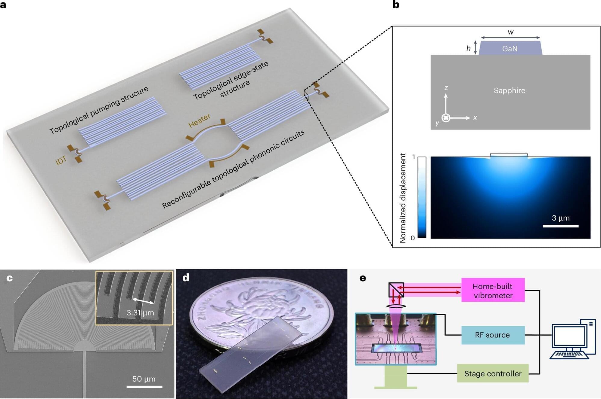
Phononic circuits are emerging devices that can manipulate sound waves (i.e., phonons) in ways that resemble how electronic circuits control the flow of electrons. Instead of relying on wires, transistors and other common electronic components, these circuits are based on waveguides, topological edge structures and other components that can guide phonons.
Phononic circuits are opening new possibilities for the development of high-speed communication systems, quantum information systems and various other technologies.
To be compatible with existing infrastructure, including current microwave communication systems, and to be used to develop highly performing quantum technologies, these circuits should ideally operate at gigahertz (GHz) frequencies. This essentially means that the sound waves they generate and manipulate oscillate billions of times per second.
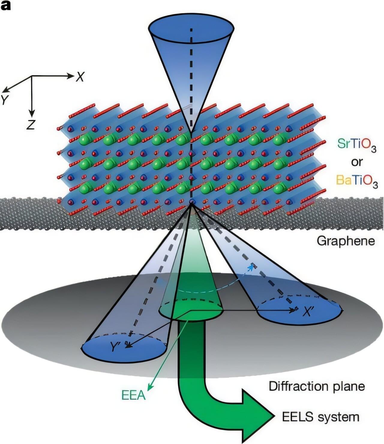
Researchers at the University of California, Irvine, together with international collaborators, have developed a new electron microscopy method that has enabled the first-ever imaging of vibrations, or phonons, in specific directions at the atomic scale.
In many crystallized materials, atoms vibrate differently along varying directions, a property known as vibrational anisotropy, which strongly influences their dielectric, thermal and even superconducting behavior. Gaining a deeper understanding of this anisotropy allows engineers to tailor materials for use in electronics, semiconductors, optics and quantum computing.
In a paper published in Nature, the UC Irvine-led team details the workings of its momentum-selective electron energy-loss spectroscopy technique and its power to unveil the fundamental lattice dynamics of functional materials.

With the rapid development of wearable electronics, neurorehabilitation, and brain-machine interfaces in recent years, there has been an urgent need for methods to conformally wrap thin-film electronic devices onto biological tissues to enable precise acquisition and regulation of physiological signals.
Conventional methods typically rely on external pressure to force devices onto conformal contact. However, when applied to uneven three-dimensional surfaces such as skin, brain, or nerves, they generate significant internal stress which can easily damage fragile metal circuits and inorganic chips. This is an obstacle to the advancement of flexible electronics.
In a study published in Science, Prof. Song Yanlin’s team from the Institute of Chemistry of the Chinese Academy of Sciences, along with collaborators from Beijing Tiantan Hospital, Nanyang Technological University, and Tianjin University, propose a new film transfer strategy named as drop-printing, which has potential applications in bioelectronics, flexible displays, and micro-/nano-manufacturing.
In a collaboration showing the power of innovation and teamwork, physicists and engineers at the Department of Energy’s Oak Ridge National Laboratory developed a mobile muon detector that promises to enhance monitoring for spent nuclear fuel and help address a critical challenge for quantum computing.
Similar to neutrons, scientists use muons, fundamental subatomic particles that travel at nearly the speed of light, to allow scientists to peer deep inside matter at the atomic scale without damaging samples. However, unlike neutrons, which decay in about 10 minutes, muons decay within a couple of microseconds, posing challenges for using them to better understand the world around us.
The new detector achieves an important step toward ensuring the safety and accountability of nuclear materials and supports the development of advanced nuclear reactors that will help address the challenges of waste management. It also acts as a key step toward developing algorithms and methods to manage errors caused by cosmic radiation in qubits, the basic units of information in quantum computing. The development of the muon detector at ORNL reflects the lab’s strengths in discovery science enabled by multidisciplinary teams and powerful research tools to address national priorities.