A gene editing technique may prevent the slaughter of animals not needed by the livestock industry.


Few developments have rocked the biotechnology world or generated as much buzz as the discovery of CRISPR-Cas systems, a breakthrough in gene editing recognized in 2020 with a Nobel Prize. But these systems that naturally occur in bacteria are limited because they can make only small tweaks to genes. In recent years, scientists discovered a different system in bacteria that might lead to even more powerful methods for gene editing, given its unique ability to insert genes or whole sections of DNA in a genome.
New research from The University of Texas at Austin dramatically expands the number of naturally occurring versions of this system, giving researchers a wealth of potential new tools for large-scale gene editing.
Other scientists had identified clusters of genes that use CRISPR to insert themselves into different places in an organism’s genome, dubbed CRISPR-associated transposons (CASTs). Earlier work has shown they can be used to add an entire gene or large DNA sequence to the genome, at least for bacteria.

Following October’s news that Jeff Bezos’ Blue Origin spaceflight company planned to build its own commercial space station in low Earth orbit, NASA announced on Thursday it has selected the program for funding through a Space Act Agreement to further develop the station’s design. The funding is part of NASA’s Commercial LEO Development program, which aims to “develop a robust commercial space economy in LEO, including supporting the development of commercially owned and operated LEO destinations.”
“We are pleased that NASA supports the development of Orbital Reef, a revolutionary approach to making Earth orbit more accessible to diverse customers and industries,” Brent Sherwood, Senior Vice President of Advanced Development Programs for Blue Origin, said in a prepared statement. The station would be an orbital “mixed-use space business park” that would offer any number of turnkey services as well as reduced operational costs for burgeoning low-g industries “in addition to meeting the ISS partners’ needs.”
Blue Origin is partnering with Sierra Space in this project with the former focusing on the architecture and infrastructure of the station — everything from its design and construction to managing lift logistics using the New Glenn heavy launch system — while the latter is tasked with developing the station’s LIFE (Large Integrated Flexible Environment). Boeing is also helping out, designing the operations-maintenance-science module and leveraging its Starliner crew capsule. Genesis Engineering Solutions is involved as well. It’s working on a single person spacecraft that tourists and employees alike will be able to putter around in.

Bongard said they found that the xenobots, which were initially sphere-shaped and made from around 3,000 cells, could replicate. But it happened rarely and only in specific circumstances. The xenobots used “kinetic replication” — a process that is known to occur at the molecular level but has never been observed before at the scale of whole cells or organisms, Bongard said.
The US scientists who created the first living robots say the life forms, known as xenobots, can now reproduce — and in a way not seen in plants and animals.
Formed from the stem cells of the African clawed frog (Xenopus laevis) from which it takes its name, xenobots are less than a millimeter (0.04 inches) wide. The tiny blobs were first unveiled in 2020 after experiments showed that they could move, work together in groups and self-heal.
Now the scientists that developed them at the University of Vermont, Tufts University and Harvard University’s Wyss Institute for Biologically Inspired Engineering said they have discovered an entirely new form of biological reproduction different from any animal or plant known to science.

Circa 2019
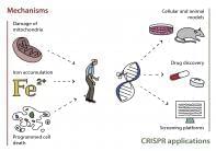
Researchers of Sechenov University and University of Pittsburgh described the most promising strategies in applying genetic engineering for studying and treating Parkinson’s disease. This method can help evaluate the role of various cellular processes in pathology progression, develop new drugs and therapies, and estimate their efficacy using animal disease models. The study was published in Free Radical Biology and Medicine.
Parkinson’s disease is a neurodegenerative disorder accompanied by a wide array of motor and cognitive impairments. It develops mostly among elderly people (after the age of 55–60). Parkinson’s symptoms usually begin gradually and get worse over time. As the disease progresses, people may have difficulty controlling their movements, walking and talking and, more importantly, taking care of themselves. Although there is no cure for Parkinson’s disease, medicines, surgical treatment, and other therapies can often relieve some symptoms.
The disease is characterized by significant (up to 50–70%) loss of dopaminergic neurons, i.e. nerve cells that synthesize neurotransmitter dopamine which enables communication between the neurons. Another hallmark is the presence of Lewy bodies — oligomeric deposits of a protein called alpha-synuclein inside the neurons.

Western intelligence agencies fear Beijing could within decades dominate all of the key emerging technologies, particularly artificial intelligence, synthetic biology and genetics.
China’s economic and military rise over the past 40 years is considered to be one of the most significant geopolitical events of recent times, alongside the 1991 fall of the Soviet Union which ended the Cold War.
MI6, depicted by novelists as the employer of some of the most memorable fictional spies from John le Carré’s George Smiley to Ian Fleming’s James Bond, operates overseas and is tasked with defending Britain and its interests.

For the first time, researchers appear to have effectively treated a genetic disorder by directly injecting a CRISPR therapy into patients’ bloodstreams — overcoming one of the biggest hurdles to curing diseases with the gene editing technology.
The therapy appears to be astonishingly effective, editing nearly every cell in the liver to stop a disease-causing mutation.
The challenge: CRISPR gives us the ability to correct genetic mutations, and given that such mutations are responsible for more than 6,000 human diseases, the tech has the potential to dramatically improve human health.

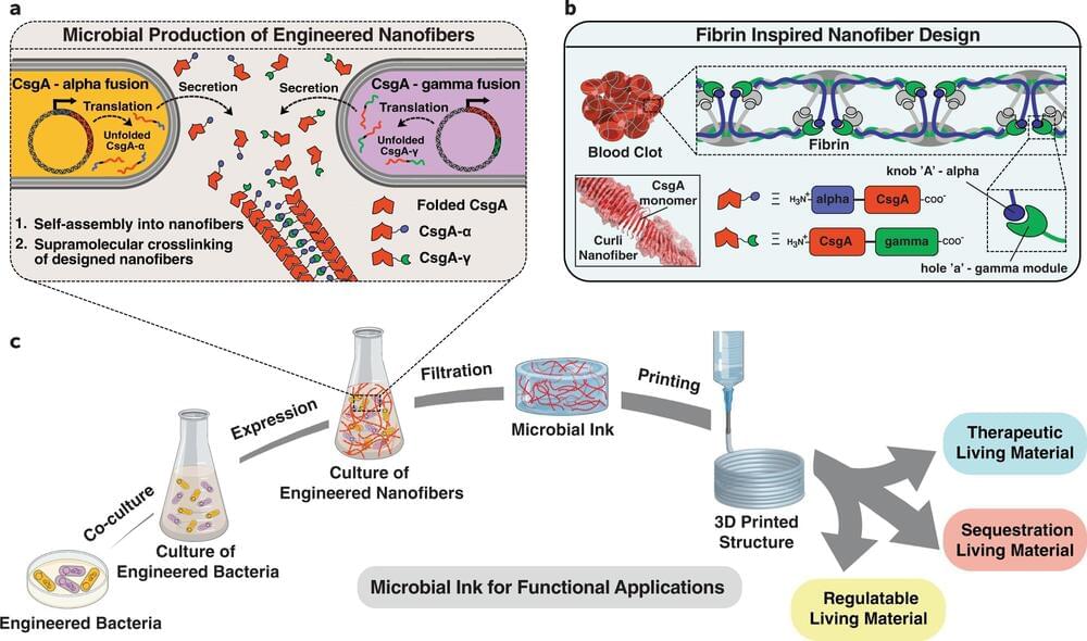
A team of researchers from Harvard University and Brigham and Women’s Hospital, Harvard Medical School, has developed a type of living ink that can be used to print living materials. In their paper published in the journal Nature Communications, the group describes how they made their ink and possible uses for it.
For several years, microbial engineers have been working to develop a means to create living materials for use in a wide variety of applications such as medical devices. But getting such materials to conform to desired 3D structures has proven to be a daunting task. In this new effort, the researchers have taken a new approach to tackling the problem—engineering Escherichia coli to produce a product that can be used as the basis for an ink for use in a 3D printer.
The work began by bioengineering the bacteria to produce living nanofibers. The researchers then bundled the fibers and added other ingredients to produce a type of living ink that could be used in a conventional 3D printer. Once they found the concept viable, the team bioengineered other microbes to produce other types of living fibers or materials and added them to the ink. They then used the ink to print 3D objects that had living components. One was a material that secreted azurin—an anticancer drug—when stimulated by certain chemicals. Another was a material that sequestered Bisphenol A (a toxin that has found its way into the environment) without assistance from other chemicals or devices.

Scientists have discovered a way to stop the COVID-19 virus from replicating in infected human cells, marking major progress towards a definitive treatment for the deadly illness and accentuating the potential of genetic engineering to cure viral diseases.
The study explores the use of CRISPR, a genome editing tool, and builds on research that started at Australia’s Peter MacCallum Cancer Center in 2019, when Dr. Mohamed Fareh and Prof. Joe Trapani showed that CRISPR could be used to eliminate abnormal RNAs that drive children’s cancers.
At the beginning of the pandemic, and in collaboration with Director Prof. Sharon Lewin and Dr. Wei Zhao from the Doherty Institute, the scientists reprogrammed the same CRISPR tool to suppress replication of the RNA virus SARS-CoV-2 — and importantly, its “variants of concern” — in a test tube model. SARS-CoV-2, which is short for Severe Acute Respiratory Syndrome Coronavirus 2, is the virus that causes COVID-19.

ROME, July 2 (Reuters) — A United Nations-backed scientific research centre has teamed up with an Italian tech firm to explore whether laser light can be used to kill coronavirus particles suspended in the air and help keep indoor spaces safe.
The joint effort between the International Centre for Genetic Engineering and Biotechnology (ICGEB) of Trieste, a city in the north of Italy, and the nearby Eltech K-Laser company, was launched last year as COVID-19 was battering the country.
They created a device that forces air through a sterilization chamber which contains a laser beam filter that pulverizes viruses and bacteria.