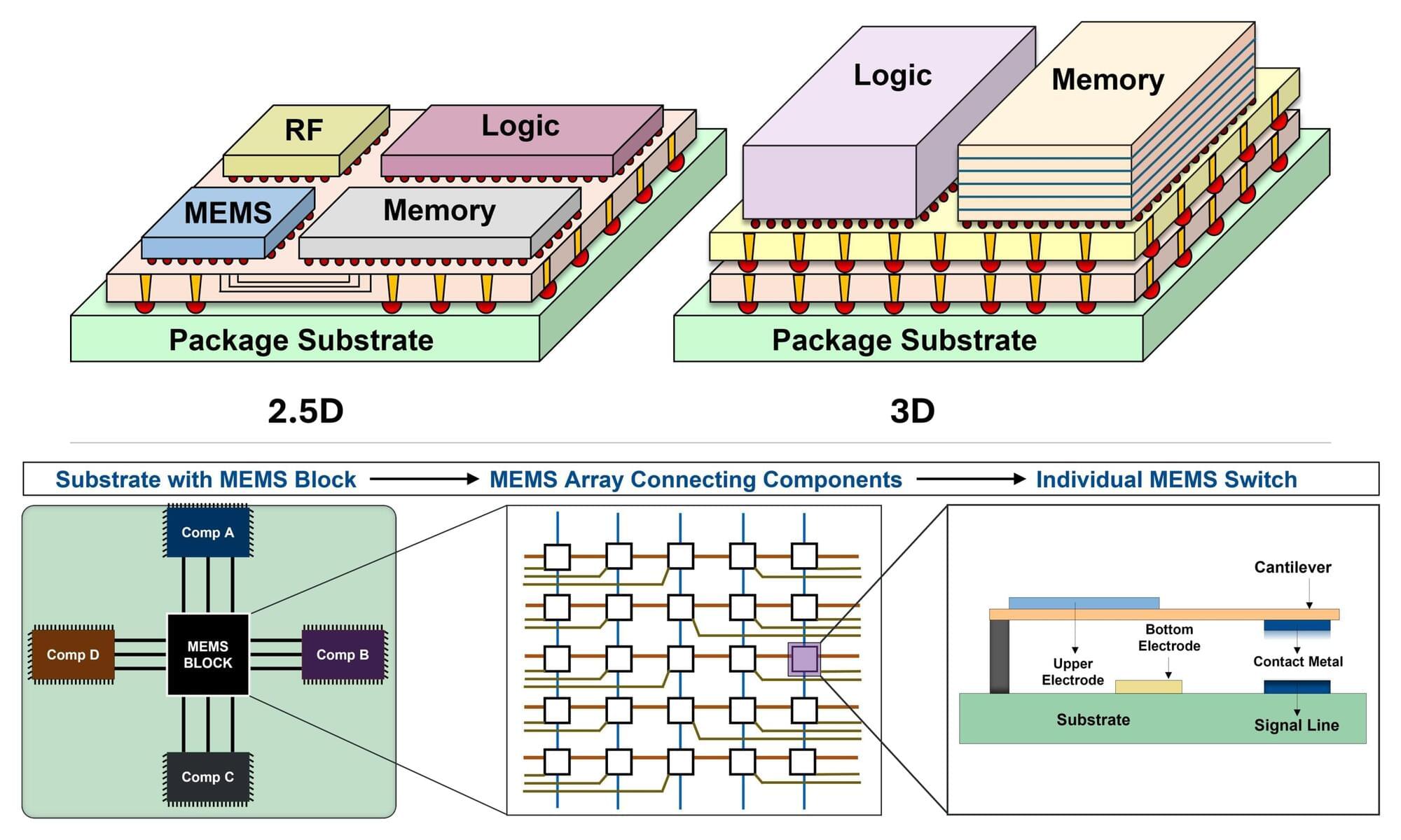
I spend my days looking inside chip packages to find out why they failed. With X-ray tomography or an acoustic microscope, I can see through a finished package without opening it: every solder bump, every copper trace, every buried layer. It is satisfying detective work. Somewhere along the way, I realized it is also exactly what a reverse engineer does.
A modern package is no longer a single chip in a plastic shell. Processors, memory and power chips, often made by different companies in different countries, sit side by side on a shared substrate, wired together by copper traces finer than a human hair. Anyone who can map those traces learns how the system is built. They can clone it, build a counterfeit or work out where to slip in a malicious modification. And the tools for that mapping, the same ones I use for failure analysis, can be bought by anyone with a budget.
This matters more every year. AI accelerators, defense electronics and critical infrastructure all depend on packages that pass through many hands (designers, foundries, assembly houses, test labs, distributors) before they are installed. Each handoff is a chance to look, copy or tamper. Most hardware security work focuses on the chips themselves. The substrate that connects them has received far less attention, even though its wiring is effectively the blueprint of the whole system.