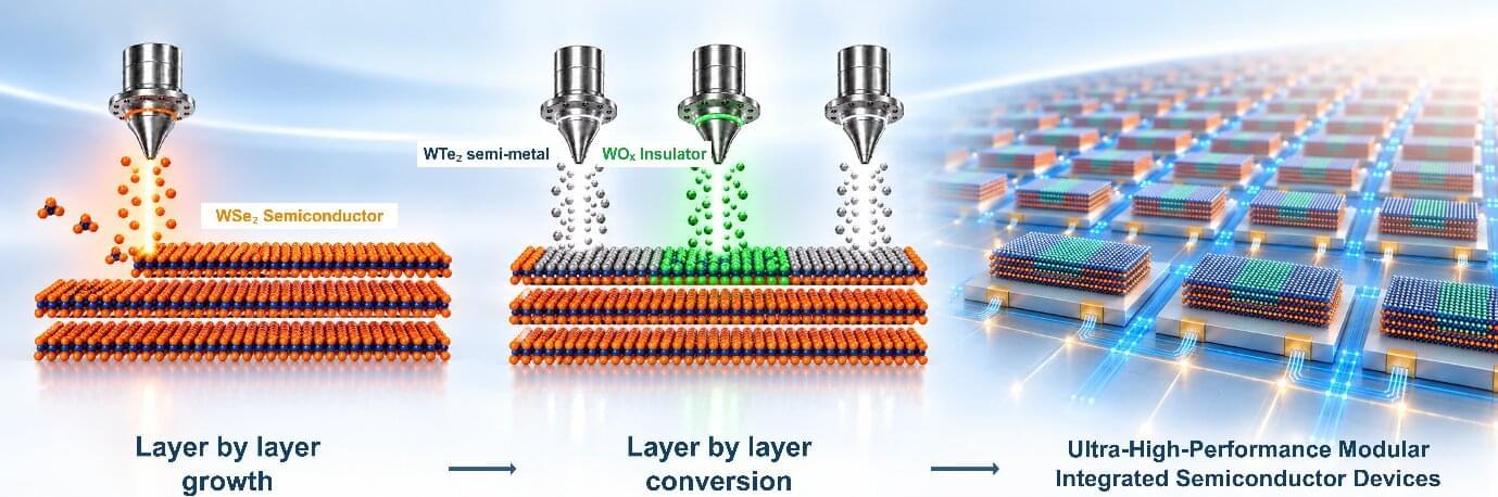
A transistor normally requires several fundamentally different materials—a semiconductor to carry current, an insulating dielectric to control it and metallic contacts through which current enters and leaves. Integrating all of these components becomes increasingly difficult as semiconductor devices approach the atomic scale.
A research team led by Director Jo Moon-Ho of the Center for Van der Waals Quantum Solids within the Institute for Basic Science (IBS) has now demonstrated a fundamentally different approach. Instead of fabricating the semiconductor, dielectric and contact materials separately and then assembling them into a device, the researchers started from a single layered crystal and chemically converted selected atomic layers and regions into the different materials needed for a working transistor. The work is published in the journal Science.