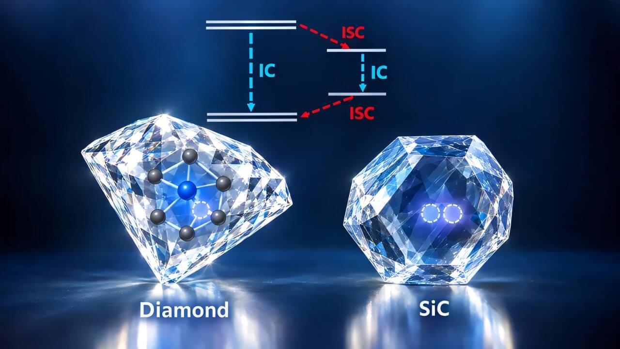
When light hits a tiny defect embedded in a solid material like diamond or silicon carbide, it can kick the defect’s electrons into an excited state. These spin defects have the potential to be used as stable, readable qubits for quantum technologies, for example, quantum sensing. But modeling the full physics of their energetics over time—a key step in developing spin defects into new technologies—is a challenging task.
Now, researchers at the University of Chicago Pritzker School of Molecular Engineering (UChicago PME) have built a computational framework that captures the full optical cycle of such spin defects, including the prediction of internal conversion, a process particularly hard to model.
Their results, published in Physical Review Letters, shed light on how to use the defects in the design of quantum materials and could also be applied to a different class of systems used in renewable energy conversion and storage.