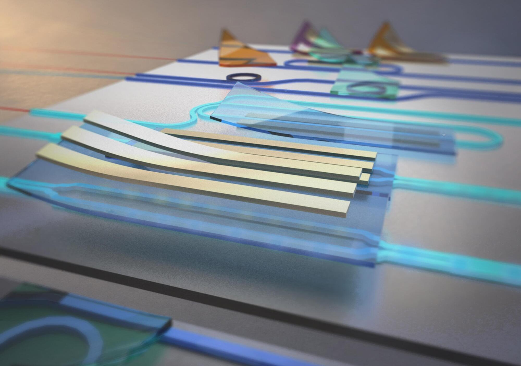
Photonic integrated circuits route information with optical signals instead of relying only on electrical currents. Silicon (Si) and silicon nitride (SiNx) are excellent photonic platforms for waveguides, but they cannot efficiently perform the ever-increasing tasks required for fully integrated optical systems. A heterogeneous photonic integration platform capable of interfacing different optical materials with high performance is thus an ongoing challenge for both academia and industry.
Conventional approaches use heteroepitaxy to realize thin-film functional materials on target optical substrates. However, this method confronts fundamental challenges in lattice matching and process compatibility, and substantially deteriorated epilayer material quality is often observed in mismatched photonic chips.
In our recent work published in Nature, a group of researchers from Washington University in St. Louis (WUSTL), the Swiss Federal Institute of Technology Lausanne (EPFL), and the Massachusetts Institute of Technology (MIT) demonstrated a different strategy: preparing desired thin-film materials on their most suitable parent substrates, then delaminating them into freestanding single-crystalline nanomembranes for unbridled heterogeneous photonic integration on arbitrary photonic templates.