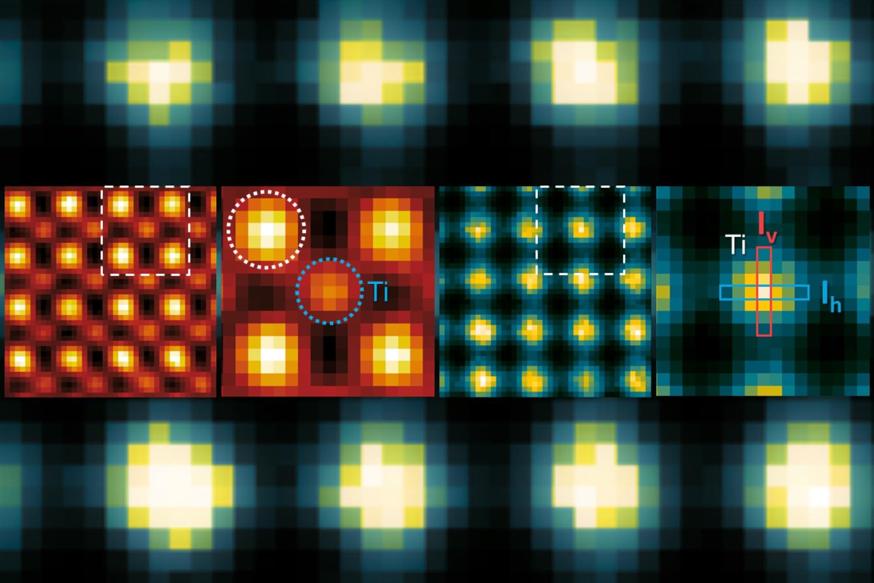
Many material properties depend on how electrons are arranged inside a material. Their distribution determines, for example, whether a material conducts electricity or displays magnetic behavior. Understanding how electrons organize themselves at the atomic scale is therefore one of the major challenges in materials science. Now, a team led by researchers at the Institute of Materials Science of Barcelona (ICMAB-CSIC) has developed a new technique that, for the first time, reveals how electrons are organized inside materials with an unprecedented level of detail.
Until now, available techniques could only provide an overall picture of electronic structure. They could not reveal in detail how electrons vary from one atom to another, either at the surface or deeper within the material. “This type of instrument is like opening a box that until now has been closed,” says Jaume Gàzquez, ICMAB-CSIC researcher and one of the corresponding authors of the paper published in Nature Materials. “We can now observe phenomena that simply could not be seen before.”
The work was carried out in collaboration with the University of the Chinese Academy of Sciences, Uppsala University (Sweden), the University of Washington (United States), and the Pacific Northwest National Laboratory (United States). The project brought together expertise in advanced microscopy, theoretical simulations and materials synthesis.