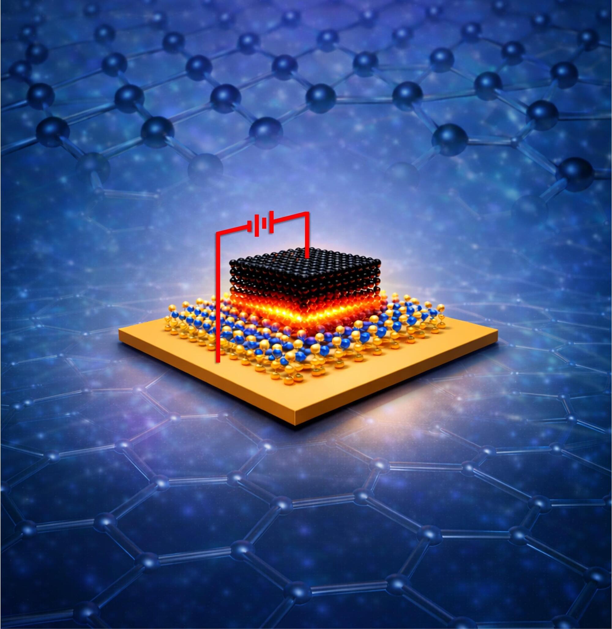
The high-performance semiconductor devices powering smartphone displays, AI computing, EV batteries and more are increasingly incorporating 2D materials to overcome silicon’s scaling limits. To optimize these technologies, a University of Michigan Engineering team developed a precise mathematical framework that accounts for anisotropic—or unevenly spreading—conductivity and device geometry.
Accurate models of how currents move through anisotropic thin films, made of layered 2D materials, can enable the design of more reliable, high-performance nanoelectric devices. Specifically, the model can help engineers reduce current crowding and spreading resistance, essentially current traffic jams, that occur at vertical electrical contacts that connect with the top of a 2D surface. The study is published in ACS Applied Electronic Materials.