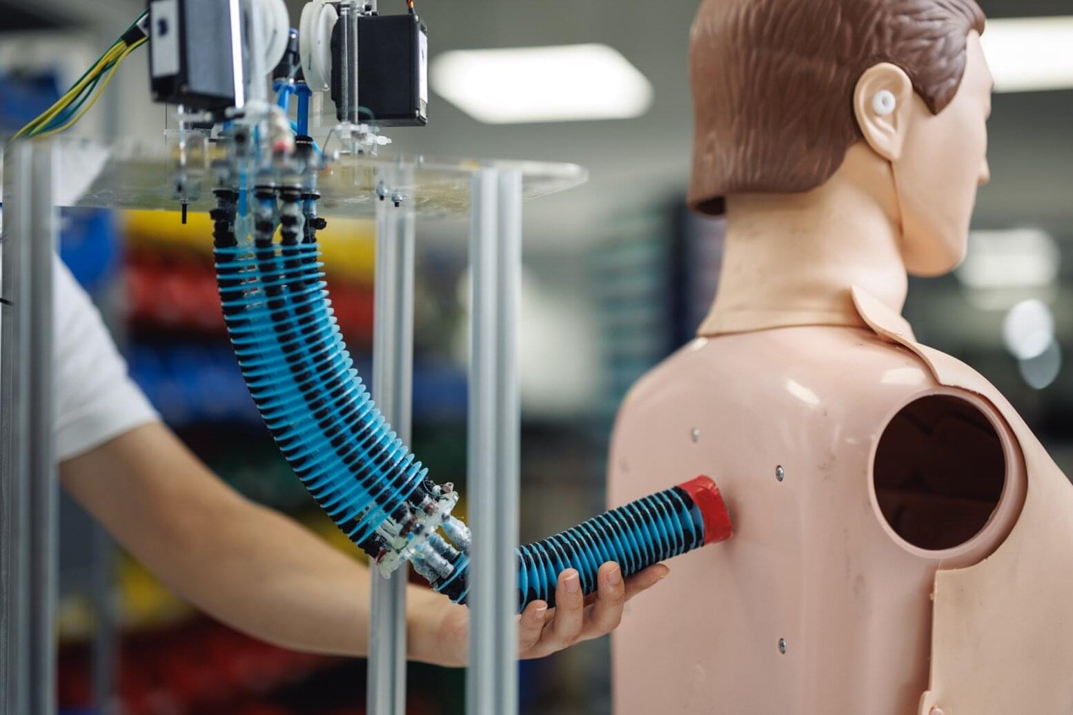
Researchers have developed an AI control system that enables soft robotic arms to learn a wide repertoire of motions and tasks once, then adjust to new scenarios on the fly without needing retraining or sacrificing functionality. This breakthrough brings soft robotics closer to human-like adaptability for real-world applications, such as in assistive robotics, rehabilitation robots, and wearable or medical soft robots, by making them more intelligent, versatile, and safe. The research team includes Singapore-MIT Alliance for Research and Technology’s (SMART) Mens, Manus & Machina (M3S) interdisciplinary research group, and National University of Singapore (NUS), alongside collaborators from Massachusetts Institute of Technology (MIT) and Nanyang Technological University (NTU Singapore).
Unlike regular robots that move using rigid motors and joints, soft robots are made from flexible materials such as soft rubber and move using special actuators—components that act like artificial muscles to produce physical motion. While their flexibility makes them ideal for delicate or adaptive tasks, controlling soft robots has always been a challenge because their shape changes in unpredictable ways. Real-world environments are often complicated and full of unexpected disturbances, and even small changes in conditions—like a shift in weight, a gust of wind, or a minor hardware fault—can throw off their movements.
Research by academics at King’s College London and the AI Objectives Institute has shed light on why what matters is not just how much of a job AI can do, but which parts. Dr. Bouke Klein Teeselink and Daniel Carey analyzed hundreds of millions of job postings across 39 countries before and after the release of ChatGPT in November 2022. They found that occupations with a large number of tasks exposed to AI automation, for example basic administration or data entry, saw a 6.1% decline in job postings on average. Importantly, however, this effect depends not only on how many tasks are exposed, but also on which tasks.
When AI automates the routine, less-skilled parts of a job, the work that remains tends to be more specialized. Fewer people can do it, so wages rise. The researchers cite the example of a human resources specialist whose administrative paperwork is now handled by AI, leaving them to focus on complex employee relations and judgment calls.
But when AI can perform the more specialized, cognitively demanding tasks, wages decrease because the job no longer requires scarce expertise. This example can apply to roles such as junior software engineers, the researchers found.
An intranasal flu antibody can protect against both influenza A and B in mice and nonhuman primates and is safe in humans, according to new preclinical experiments and two phase one clinical trials published in Science TranslationalMedicine.
Intranasal CR9114 is safe in humans, and twice-daily dosing confers protection against influenza virus challenge in macaques.
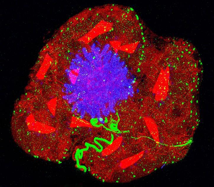
Expansion microscopy is possible for any lab with a basic microscope. Specific biomolecules such as proteins are anchored to a hydrogel. As the gel absorbs added water, it swells and the space between the anchor points dilates. This allows researchers to visualize extra-tiny anatomy or see inside cells with tough barriers.
How physically magnifying objects using a key ingredient in diapers has opened an unprecedented view of the microbial world.
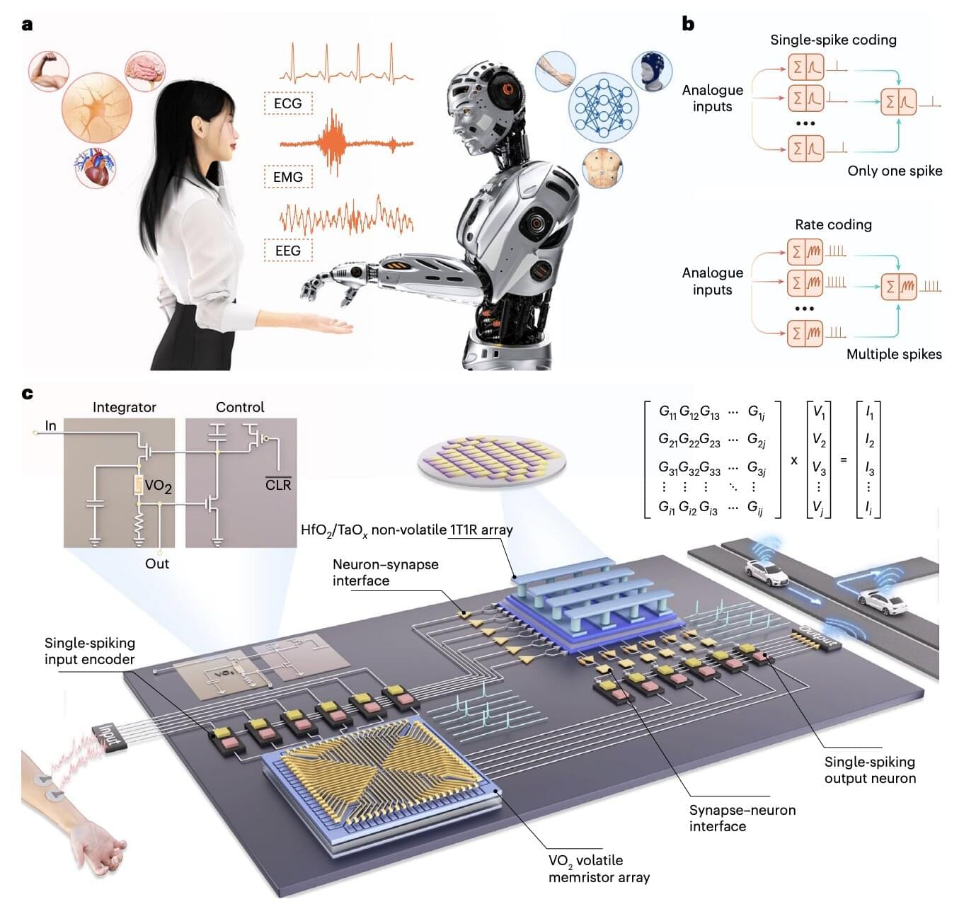
The use of artificial intelligence (AI) systems, such as the models underpinning the functioning of ChatGPT and various other online platforms, has grown exponentially over the past few years. Current hardware and electronic devices, however, might not be best suited for running these systems, which are computationally intensive and can drain huge amounts of energy.
Electronics engineers worldwide have thus been trying to develop alternative hardware that better reflects how the human brain processes information and could thus run AI systems more reliably, while consuming less power. Many of these brain-inspired hardware systems rely on memristors, electronic components that can both store and process information.
Researchers at Peking University and Southwest University recently introduced a new neuromorphic hardware system that combines different types of memristors. This system, introduced in a paper published in Nature Electronics, could be used to create new innovative brain-machine interfaces and AI-powered wearable devices.
Joscha Bach explores the nature of consciousness, free will, and reality through the lens of computation, cognitive science, and philosophy. Rather than treating the mind as a mystical entity, Joscha frames consciousness as a constructed dream—a model generated by the brain to make sense of the world and coordinate behavior.
We examine why beliefs should remain provisional, how the self functions as a useful fiction, and why suffering emerges when internal learning signals misfire. Joscha explains why free will feels real even if decisions arise before awareness, how meaning exists beyond the individual ego, and why wisdom is not simply knowledge but the ability to orient oneself within larger systems of value.
André’s Book Recs: https://www.knowthyselfpodcast.com/bo… 00:00 Intro: Joscha Bach 04:24 Agnosticism, Evidence, and Logical Alternatives 11:20 Reality as a Mental Simulation 13:00 What Physicalism Actually Claims 16:55 Telepathy, Rituals, and Distributed Minds 19:45 Consciousness Does Not Make Decisions 22:55 Free Will as a Post-Hoc Story 24:00 Consciousness as a Trance State 26:00 Meditation and the Illusion of Self 29:10 Out-of-Body Experiences Explained 31:07 Ad: BON CHARGE 36:30 Why the Brain Fills in Missing Reality 39:50 Dreams, Selves, and Narrative Identity 43:20 Intelligence, Models, and World-Building 47:10 Why Reality Feels Stable 51:00 Meaning, Agency, and Mental Compression 55:10 Why Consciousness Feels Central (But Isn’t) 59:30 The Psychological World vs Physical Reality 1:04:10 Intelligence Without Awareness 1:08:45 The Cost of Believing the Self Is Real 1:13:30 Waking Up From the Narrative 1:18:40 What a Cognitive Science View Really Implies 1:23:30 Final Thoughts: Living Inside the Dream ___________ Episode Resources: https://www.cimc.ai/ / andreduqum / knowthyself / @knowthyselfpodcasthttps://www.knowthyselfpodcast.com Listen to the show: Spotify: https://spoti.fi/4bZMq9l Apple: https://apple.co/4iATICX
___________ 00:00 Intro: Joscha Bach. 04:24 Agnosticism, Evidence, and Logical Alternatives. 11:20 Reality as a Mental Simulation. 13:00 What Physicalism Actually Claims. 16:55 Telepathy, Rituals, and Distributed Minds. 19:45 Consciousness Does Not Make Decisions. 22:55 Free Will as a Post-Hoc Story. 24:00 Consciousness as a Trance State. 26:00 Meditation and the Illusion of Self. 29:10 Out-of-Body Experiences Explained. 31:07 Ad: BON CHARGE 36:30 Why the Brain Fills in Missing Reality. 39:50 Dreams, Selves, and Narrative Identity. 43:20 Intelligence, Models, and World-Building. 47:10 Why Reality Feels Stable. 51:00 Meaning, Agency, and Mental Compression. 55:10 Why Consciousness Feels Central (But Isn’t) 59:30 The Psychological World vs Physical Reality. 1:04:10 Intelligence Without Awareness. 1:08:45 The Cost of Believing the Self Is Real. 1:13:30 Waking Up From the Narrative. 1:18:40 What a Cognitive Science View Really Implies. 1:23:30 Final Thoughts: Living Inside the Dream. ___________
Philosopher, computer scientist, and AI developer Joscha Bach explains his interest in animist ideas about spirits governing reality and how they exist as’software patterns’.
Liu et al. reveal that BIW negatively regulates BR signaling by promoting BZR1 ubiquitination and degradation, while BIN2 enhances BIW’s stability and activity. Through the BZR1-dependent pathway, BIW inhibits lateral root development and chilling tolerance in tomato, providing a strategy for developing elite crop germplasm by targeted manipulation of BIW.


