Discover the world’s best science and medicine | Nature.com

Discover the world’s best science and medicine | Nature.com
“It’s not a true aspiration catheter, but it can work,” says Sillero. “We have to be careful because the groin is very small at this age — you have to really think outside the box.”
Neurosurgical procedures are especially challenging when operating on kids under two, he explains, partly because medical supply companies don’t make miniature versions of devices such as catheters, since paediatric stroke and aneurysm (a bulge in a blood vessel) are so rare.
Sillero has overcome such challenges not only through improvisation, but thanks to Children’s Health’s innovative model for diagnosis and treatment, which encourages close collaboration between different specialists.
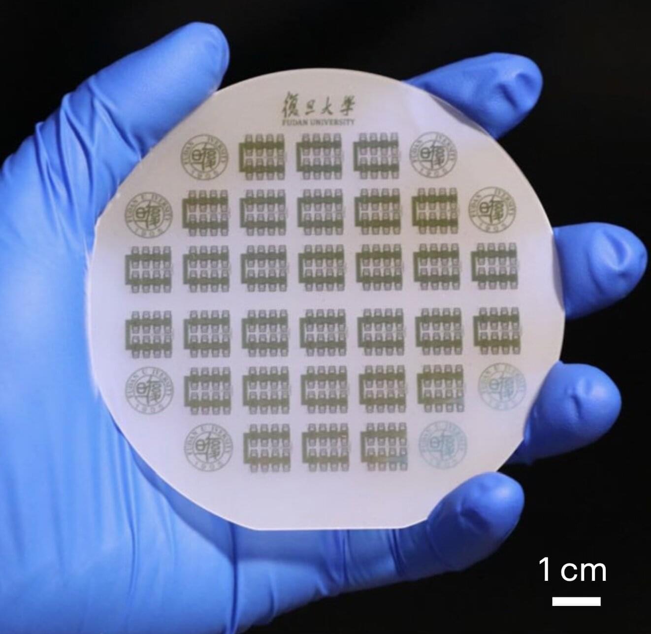
Two-dimensional (2D) semiconductors, materials that can conduct electricity and are only a few atoms thick, are promising alternatives to the conventional silicon-based semiconductors currently used to fabricate many electronics. Despite their promise, these materials have not yet been deployed on a large scale.
One reason for this is that reliably synthesizing them and patterning them to produce wafers (i.e., circular substrates employed in the manufacturing of electronics) has so far proved challenging. In fact, many existing patterning techniques rely on chemical processes or polymer masks, both of which can leave unwanted residues on a wafer or damage the surface of 2D semiconductors.
Researchers at Nanyang Technological University recently developed a new strategy to pattern 2D films into high-quality wafer-scale arrays, without damaging them or introducing undesirable residues. Their proposed method, outlined in a paper published in Nature Electronics, entails the use of a metal stamp producing three-dimensional (3D) patterns, which can be pressed onto 2D materials to produce a wafer with desired patterns.
As artificial intelligence (AI) rapidly advances, the physical limitations of conventional semiconductor hardware have become increasingly apparent. AI models today demand vast computational resources, high-speed processing, and extreme energy efficiency—requirements that traditional silicon-based systems struggle to meet. However, nanotechnology is stepping in to reshape the future of AI by offering solutions that are faster, smaller, and smarter at the atomic scale.
The recent article published by AZoNano provides a compelling overview of how nanotechnology is revolutionizing the design and operation of AI systems, pushing beyond the constraints of Moore’s Law and Dennard scaling. Through breakthroughs in neuromorphic computing, advanced memory devices, spintronics, and thermal management, nanomaterials are enabling the next generation of intelligent systems.
Perovskites have long captivated the interest of materials scientists and engineers for their remarkable potential in next-generation solar cells, LEDs, and optoelectronic devices. Now, a newly published study pushes the envelope even further by showing how carefully applied pressure can finely tune the light-handling properties of a 2D hybrid perovskite, marking a significant leap toward real-time structural control in photonic technologies.
The research, carried out using the Canadian Light Source (CLS) at the University of Saskatchewan and the Advanced Photon Source (APS) in Chicago, utilized ultrabright synchrotron radiation to observe how perovskite layers respond under pressure. The focus was a 2D Dion–Jacobson hybrid lead iodide perovskite with alternating organic and inorganic sheets—structures whose interaction defines how the material absorbs, emits, or modulates light.
Oral microbiota dysbiosis and altered salivary cortisol levels have been linked to depression and anxiety. Given that bacterial transmission can occur between spouses, this study aimed to investigate whether the transmission of oral microbiota between newlywed couples mediates symptoms of depression and anxiety.
An imaging method provides unprecedented resolution for studies of quantum materials by relying on superconductors’ extreme sensitivity to light.
The energy deposited in a superconductor by a single photon can register a detectable signal, which is why superconductors are employed in some extremely sensitive detectors. Now researchers have shown how to use this sensitivity to create maps of the superconducting properties of a material with nanometer resolution [1]. The technique can also detect polaritons—hybrid light–matter excitations that may be useful in quantum technologies—with higher resolution than earlier methods. The researchers expect the new technique to be useful in fields as diverse as quantum information and nanophotonics.
When a superconductor held just below its critical temperature absorbs a single photon, the superconductivity can be destroyed in a small region of the material, triggering a small electrical signal. Recent advances have expanded the operating temperatures of such detectors and improved their sensitivities to photons over a wide range of frequencies, enabling many new applications. Mengkun Liu of Stony Brook University in New York and colleagues wondered if the same sensitivity might be employed to build high-resolution spatial maps of the properties of superconducting samples. “Spatial variations often influence superconducting strength and coherence, so an ability to image these properties locally would bring valuable insight,” says Stony Brook team member Ran Jing.
Many quantum technologies function only at ultralow temperatures. Managing the flow of heat in these systems is crucial for protecting their sensitive components. Now Matteo Pioldi and his colleagues at the CNR Institute of Nanoscience and the Scuola Normale Superiore, both in Pisa, Italy, have devised a thermal analogue of a transistor that could facilitate this heat management [1]. Just as a transistor can control electric currents, the new device has the potential to control heat currents in cryogenic quantum systems.
The most common type of transistor has three electrical terminals: the source, the gate, and the drain. Adjusting the voltage applied to the gate alters the strength of the electric current flowing from the source to the drain. In the proposed device, a semiconductor-based thermal reservoir serves as the source, and metallic thermal reservoirs serve as the gate and the drain. A second semiconductor-based reservoir exchanges heat with the source through photons and with the gate and the drain through electrons. Changing the gate’s temperature affects how easily heat flows through the device and, in turn, alters the strength of the heat current flowing from the source to the drain.
Pioldi and his colleagues performed numerical simulations of their device in a realistic setup at ultralow temperatures. They found that a small change in the strength of the heat current coming from the gate could cause the strength of the current between the source and the drain to increase by an amount that was 15 times larger. They say that their device could improve heat management in quantum circuits and thus help optimize quantum sensors, quantum computers, and other temperature-sensitive quantum systems.
Using ultrafast x-ray pulses, researchers have probed the chirality of spin spirals in synthetic antiferromagnets.
Magnetism is a constant companion in our daily lives. Data storage, sensors, electric motors—none of these devices would function without it. Yet most technologies exploit only the simplest form of magnetic order: ferromagnetism, in which all magnetic moments within a domain align in the same direction. But magnetic order can be far more intricate. In conventional antiferromagnets (AFMs), the magnetic moments align in opposite directions to produce zero net magnetization, a type of order which has several advantages over ferromagnetism in many next-generation technological applications. In more exotic materials, the magnetic moments can twist into spirals, vortices, and other spin structures that might one day be used to store information. Occurring in both ferromagnets and AFMs, these spin structures are defined by their chirality, the direction in which the spins rotate relative to a fixed axis.
The chirality is a key fingerprint of the competing interactions at play in complex magnetic systems. However, observing the dynamics of chirality and magnetization in AFMs has been experimentally challenging, as both can evolve over nanometer length scales and on femtosecond timescales. In a new study, Zongxia Guo from the French National Centre for Scientific Research and colleagues have taken a major step forward by probing both quantities with ultrashort and ultrabright pulses from a free-electron laser (FEL) [1]. The researchers look specifically at spin spirals in an AFM, and they find that—under laser excitation—the chirality and magnetization evolve together in near unison and on significantly faster time scales than is observed for ferromagnets. Such fast spin dynamics in chiral spin structures offers a promising new route for how we will store, transfer, and compute information in the future.