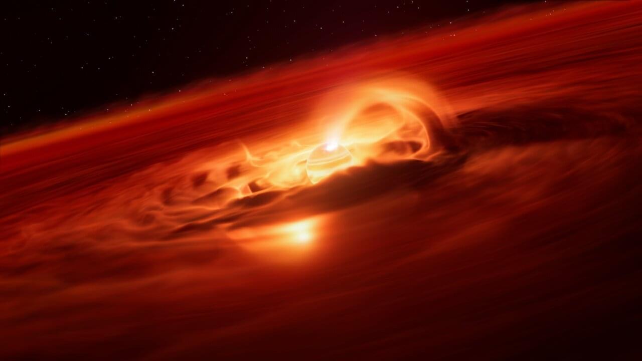
The IGDA says the problem isn’t the rules themselves, but their “vague” enforcement.

The Dutch chip equipment manufacturer will be exempted from the new US tariffs, allowing chipmakers like TSMC and Samsung easy access to lithography machines in America.
Well, the US and EU recently concluded on a trade deal, setting the tariff rates to the “baseline” 15% figure, along with potential ‘hundreds of billions’ in investments by the EU into America’s energy sector. However, there are tariff exemptions with specific categories, and one of them includes semiconductors, according to a statement released by the European Commission. This means that US companies could import chip equipment and essentials into the nation without paying the extra costs to the government in form of tariffs, and this means great news for the likes of Samsung and TSMC.
Discover the world’s best science and medicine | Nature.com
“It’s not a true aspiration catheter, but it can work,” says Sillero. “We have to be careful because the groin is very small at this age — you have to really think outside the box.”
Neurosurgical procedures are especially challenging when operating on kids under two, he explains, partly because medical supply companies don’t make miniature versions of devices such as catheters, since paediatric stroke and aneurysm (a bulge in a blood vessel) are so rare.
Sillero has overcome such challenges not only through improvisation, but thanks to Children’s Health’s innovative model for diagnosis and treatment, which encourages close collaboration between different specialists.
Two-dimensional (2D) semiconductors, materials that can conduct electricity and are only a few atoms thick, are promising alternatives to the conventional silicon-based semiconductors currently used to fabricate many electronics. Despite their promise, these materials have not yet been deployed on a large scale.
One reason for this is that reliably synthesizing them and patterning them to produce wafers (i.e., circular substrates employed in the manufacturing of electronics) has so far proved challenging. In fact, many existing patterning techniques rely on chemical processes or polymer masks, both of which can leave unwanted residues on a wafer or damage the surface of 2D semiconductors.
Researchers at Nanyang Technological University recently developed a new strategy to pattern 2D films into high-quality wafer-scale arrays, without damaging them or introducing undesirable residues. Their proposed method, outlined in a paper published in Nature Electronics, entails the use of a metal stamp producing three-dimensional (3D) patterns, which can be pressed onto 2D materials to produce a wafer with desired patterns.
As artificial intelligence (AI) rapidly advances, the physical limitations of conventional semiconductor hardware have become increasingly apparent. AI models today demand vast computational resources, high-speed processing, and extreme energy efficiency—requirements that traditional silicon-based systems struggle to meet. However, nanotechnology is stepping in to reshape the future of AI by offering solutions that are faster, smaller, and smarter at the atomic scale.
The recent article published by AZoNano provides a compelling overview of how nanotechnology is revolutionizing the design and operation of AI systems, pushing beyond the constraints of Moore’s Law and Dennard scaling. Through breakthroughs in neuromorphic computing, advanced memory devices, spintronics, and thermal management, nanomaterials are enabling the next generation of intelligent systems.
Perovskites have long captivated the interest of materials scientists and engineers for their remarkable potential in next-generation solar cells, LEDs, and optoelectronic devices. Now, a newly published study pushes the envelope even further by showing how carefully applied pressure can finely tune the light-handling properties of a 2D hybrid perovskite, marking a significant leap toward real-time structural control in photonic technologies.
The research, carried out using the Canadian Light Source (CLS) at the University of Saskatchewan and the Advanced Photon Source (APS) in Chicago, utilized ultrabright synchrotron radiation to observe how perovskite layers respond under pressure. The focus was a 2D Dion–Jacobson hybrid lead iodide perovskite with alternating organic and inorganic sheets—structures whose interaction defines how the material absorbs, emits, or modulates light.