As a child, you develop a sense of what “fairness” means. It’s a concept that you learn early on as you come to terms with the world around you. Something either feels fair or it doesn’t.
But increasingly, algorithms have begun to arbitrate fairness for us. They decide who sees housing ads, who gets hired or fired, and even who gets sent to jail. Consequently, the people who create them—software engineers—are being asked to articulate what it means to be fair in their code. This is why regulators around the world are now grappling with a question: How can you mathematically quantify fairness?
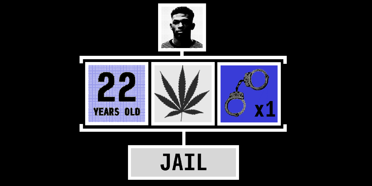
This story attempts to offer an answer. And to do so, we need your help. We’re going to walk through a real algorithm, one used to decide who gets sent to jail, and ask you to tweak its various parameters to make its outcomes more fair. (Don’t worry—this won’t involve looking at code!)