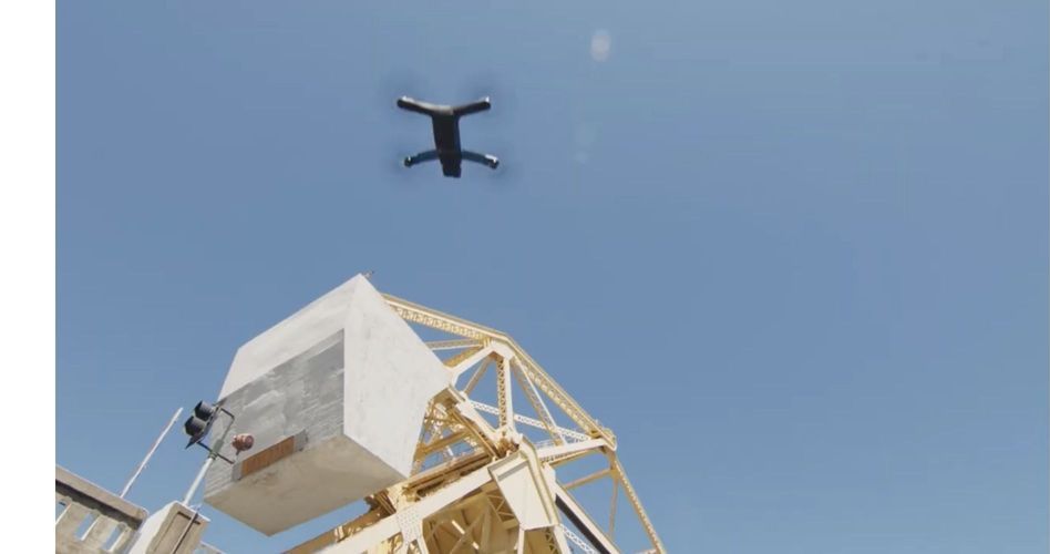
The FAA has given a green light to Beyond Visual Line of Sight flights while conducting bridge inspections in North Carolina. That’s great news for Skydio.
The FAA has given a green light to Beyond Visual Line of Sight flights while conducting bridge inspections in North Carolina. That’s great news for Skydio.
Tesla apparently has a new strategy for dealing with journalists: Don’t deal with them at all.
The electric car giant has dissolved its global public relations team, leaving the press with no formal point of contact at the world’s most valuable automaker, a new report says.
Essentially every staffer who used to work in Tesla’s PR office has either moved to a different position at the company or left altogether, according to electric vehicle industry blog Electrek, which said the move to disband the department was confirmed “at the highest level at Tesla.”
Scientists have re-investigated a sixty-year-old idea by an American physicist and provided new insights into the quantum world.
The research, which took seven years to complete, could lead to improved spectroscopic techniques, laser techniques, interferometric high-precision measurements and atomic beam applications.
Quantum physics is the study of everything around us at the atomic level, atoms, electrons and particles. Atoms and electrons which are so small, one billion placed side by side could fit within a centimeter. Because of the way atoms and electrons behave, scientists describe their behavior as like waves.
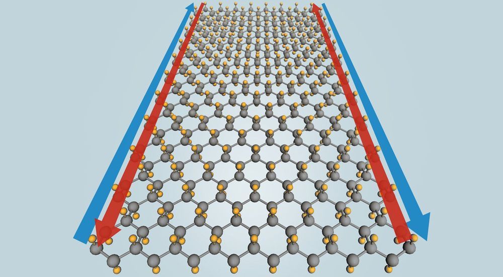
Move over, graphene and carbyne — stanene, with 100% electrical efficiency at temperatures up to 100 degrees Celsius (212F), is here, and it wants to replace the crummy, high-resistance copper wires that are a big limiting factor in current computer chips. Where graphene is a single-atom-thick layer of carbon, stanene is a single-atom-thick layer of tin.

O,.o.
AMD has patented Infinity Cache, lending credence to the rumors of its existence.
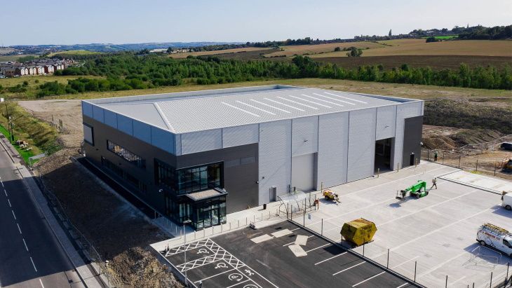
Harworth Group plc has announced the completion of the UK Atomic Energy Authority’s (UKAEA’s) new nuclear fusion technology research facility at the Advanced Manufacturing Park in Rotherham, South Yorkshire. When it opens later this year, the 2500-square-metre facility will develop and test joining technologies for fusion materials and components, including novel metals and ceramics.
Property developer Harworth said completion of the GBP22 million (USD28 million) Fusion Technology facility triggers UKAEA’s 20-year lease with Harworth at a rent in line with other manufacturers at the Advanced Manufacturing Park. UKAEA will now prepare the building prior to taking formal occupation of it later this year.
The new facility is being funded as part of the government’s Nuclear Sector Deal delivered through the Department for Business, Energy and Industrial Strategy. An additional GBP2 million of investment came from Sheffield City Region’s Local Growth Fund.
Circa 2017
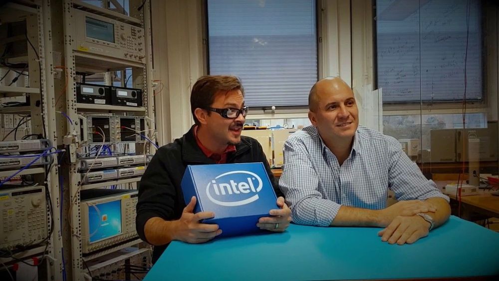
Quantum computing is the next big technological revolution, and it’s coming sooner than you might think. IBM unveiled its own quantum processor this past May, scientists have been experimenting with silicon-laced diamonds (and basic silicon, too) as a quantum computing substrate, Google is already looking at cloud-based solutions and Microsoft is already creating a new coding language for the technology. Now Intel has taken another big step towards a quantum computing reality: the company has created a new superconducting chip using advanced material science and manufacturing techniques, and delivered it to Intel’s research partner in the Netherlands, QuTech.
O,.o.
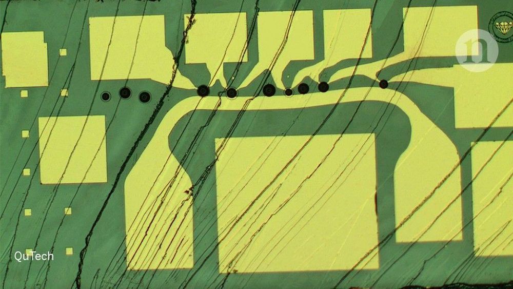
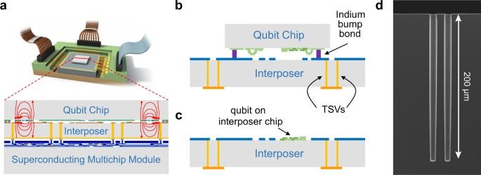
As superconducting qubit circuits become more complex, addressing a large array of qubits becomes a challenging engineering problem. Dense arrays of qubits benefit from, and may require, access via the third dimension to alleviate interconnect crowding. Through-silicon vias (TSVs) represent a promising approach to three-dimensional (3D) integration in superconducting qubit arrays—provided they are compact enough to support densely-packed qubit systems without compromising qubit performance or low-loss signal and control routing. In this work, we demonstrate the integration of superconducting, high-aspect ratio TSVs—10 μm wide by 20 μm long by 200 μm deep—with superconducting qubits. We utilize TSVs for baseband control and high-fidelity microwave readout of qubits using a two-chip, bump-bonded architecture. We also validate the fabrication of qubits directly upon the surface of a TSV-integrated chip. These key 3D-integration milestones pave the way for the control and readout of high-density superconducting qubit arrays using superconducting TSVs.

At 870 degrees Fahrenheit and 90 times Earth’s atmospheric pressure, we’re going to need something a little more robust than your Macbook to run future rovers.
Humanity has sent four rovers to Mars, and worldwide there are four more missions in the works to continue populating the red planet with robotic explorers. Why haven’t we sent a rover to Venus, our other next door planetary neighbor? Because the caustic surface of Venus will incinerate electronics with its 872º F temperatures and seize mechanical components with its immense atmospheric pressures. At 90 times the surface pressure of Earth, the surface of Venus is the equivalent of being almost 3,000 feet underwater.
The Great Galactic Ghoul might devour half the spacecraft we send to Mars, but Venus torched any ghouls living there long ago.
Fortunately, NASA recently took a big step toward achieving the dream of a Venusian rover. As reported by Ars Technica, researchers at the NASA Glenn Research Center built a computer chip that survived Venus-like conditions for an impressive 521 hours, almost 22 days. Even then, the experiment had to end not because the chip was breaking down, but because the Glenn Extreme Environments Rig (GEER) —the chamber that maintains simulated Venus temperatures and pressures—needed to be shut down after running for over three weeks straight.