This is a short summary talk by Ivan Kroupin (https://scholar.google.com/citations?user=XjxueRYAAAAJ&hl=en) and Tian Chen Zeng (https://www.researchgate.net/…
Get the latest international news and world events from around the world.
Studying the physics of sci-fi novel Ringworld by Larry Niven
Science students and academics wrote papers about the mathematics and physics of Ringworld after it was published. Larry Niven discusses whether this would happen if Ringworld was published today.
–
Learn more ➤ https://www.newscientist.com/article/.…
Subscribe ➤ https://bit.ly/NSYTSUBS
Get more from New Scientist:
Official website: https://bit.ly/NSYTHP
Facebook: https://bit.ly/NSYTFB
Twitter: https://bit.ly/NSYTTW
Instagram: https://bit.ly/NSYTINSTA
LinkedIn: https://bit.ly/NSYTLIN
About New Scientist:
New Scientist was founded in 1956 for “all those interested in scientific discovery and its social consequences”. Today our website, videos, newsletters, app, podcast and print magazine cover the world’s most important, exciting and entertaining science news as well as asking the big-picture questions about life, the universe, and what it means to be human.
New Scientist.
https://www.newscientist.com/


Scientists Tweaked LSD’s Molecular Structure and Created a Wild New Brain Drug
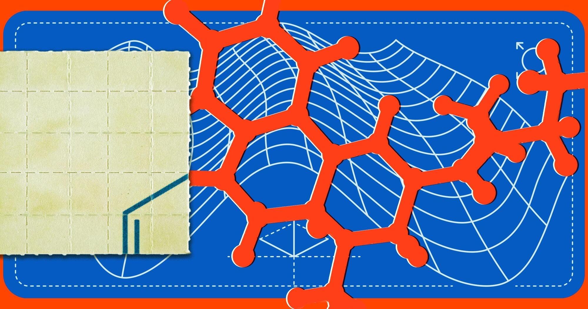
A team of researchers at the University of California, Davis, made small tweaks to the molecular structure of lysergic acid diethylamide (LSD) to see if it could be turned into an effective brain-healing treatment for patients that suffer from conditions like schizophrenia — without risking a potentially disastrous acid trip.
As detailed in a new paper published in the journal Proceedings of the National Academy of Sciences last month, the researchers created a new compound called JRT by shifting the position of just two atoms of the psychedelic’s molecular structure.
With the two atoms flipped, the new drug could still stimulate brain cell growth and repair damaged neural connections, while simultaneously minimizing psychedelic effects, in mice.


Common analgesic gas aids in opening of blood-brain barrier
Nitrous oxide, a commonly used analgesic gas, temporarily improved the opening of the blood-brain barrier (BBB) to allow gene therapy delivery in mouse models using focused ultrasound (FUS), UT Southwestern Medical Center researchers report in a new study. Their findings, published in Gene Therapy, could eventually lead to new ways to treat a variety of brain diseases and disorders.
“The approach we explored in this study has the potential to advance care for diseases of the brain that can be treated by targeted therapeutic delivery,” said study leader Bhavya R. Shah, M.D., Associate Professor of Radiology, Neurological Surgery, and in the Advanced Imaging Research Center at UT Southwestern. He’s also an Investigator in the Peter O’Donnell Jr. Brain Institute and a member of the Center for Alzheimer’s and Neurodegenerative Diseases. Deepshikha Bhardwaj, Ph.D., Senior Research Associate at UTSW, was the study’s first author.
The BBB is a highly selective border of semipermeable cells that line tiny blood vessels supplying blood to the brain. It is thought to have developed during evolution to protect the brain from toxins and infections in the blood. However, the BBB also impedes the delivery of drugs that could be used to treat neurologic or neuropsychiatric conditions, such as Alzheimer’s disease, multiple sclerosis, or brain tumors. Consequently, researchers have worked for decades to develop solutions that can temporarily open the BBB to allow treatments to enter.

Historic quantum physics breakthrough reveals what an electron really looks like
In a discovery that’s already turning heads in the scientific world, a team of physicists has achieved what was once thought impossible: they’ve measured the actual shape of a moving electron. This leap forward could not only reshape how we understand matter at the smallest scale—it might also unlock a new era of smarter, faster, and more energy-efficient electronics.


Researchers Used a One-Atom Quantum Computer to Simulate Real Molecules Over Time
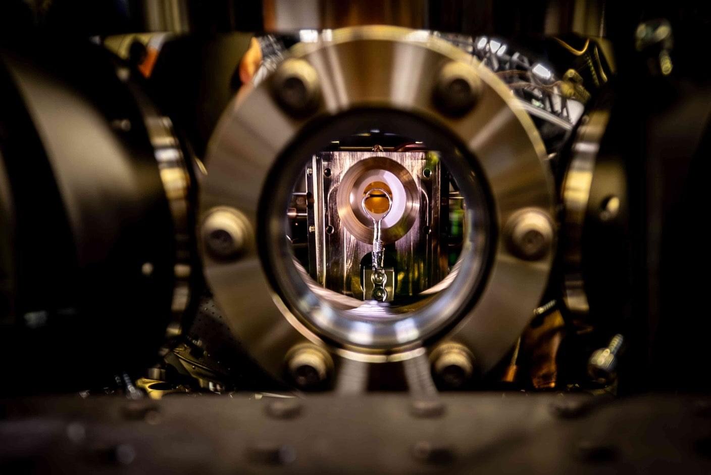
We also simulated “open-system” dynamics, where the molecule interacts with its environment. This is typically a much harder problem for classical computers.
By injecting controlled noise into the ion’s environment, we replicated how real molecules lose energy. This showed environmental complexity can also be captured by quantum simulation.

OpenAI’s Chief Scientist: AI Could Produce Novel Research by the End of the Decade
Jakub Pachocki, OpenAI’s chief scientist since 2024, believes artificial intelligence models will soon be capable of producing original research and making measurable economic impacts. In a conversation with Nature, Pachocki outlined how he sees the field evolving — and how OpenAI plans to balance innovation with safety concerns.
Pachocki, who joined OpenAI in 2017 after a career in theoretical computer science and competitive programming, now leads the firm’s development of its most advanced AI systems. These systems are designed to tackle complex tasks across science, mathematics, and engineering, moving far beyond the chatbot functions that made ChatGPT a household name in 2022.