Google inks historic US deal to buy Gen IV nuclear power for data centers.
Google inks first-ever U.S. utility deal for a Gen IV nuclear plant, as AI-driven energy needs revive interest in small modular reactors.
Google inks historic US deal to buy Gen IV nuclear power for data centers.
Google inks first-ever U.S. utility deal for a Gen IV nuclear plant, as AI-driven energy needs revive interest in small modular reactors.
Frozen tofu inspires US scientists to create reusable ‘jelly ice’ that never melts.
Interestingly, the jelly ice is 90% water and can be molded into different shapes.
“Compared to regular ice of the same shape and size, jelly ice has up to 80% of the cooling efficiency — the amount of heat the gel can absorb through phase change,” said Jiahan Zou, the study researcher.
“And we can reuse the material and maintain the heat absorbance across multiple freeze-thaw cycles, so that’s an advantage compared to regular ice,” added Zou.
Water-cooled computer mounted on wall brings steampunk art to life.
Billet Labs’ latest wall-mounted PC mod blends Victorian steampunk design with modern high-end hardware.

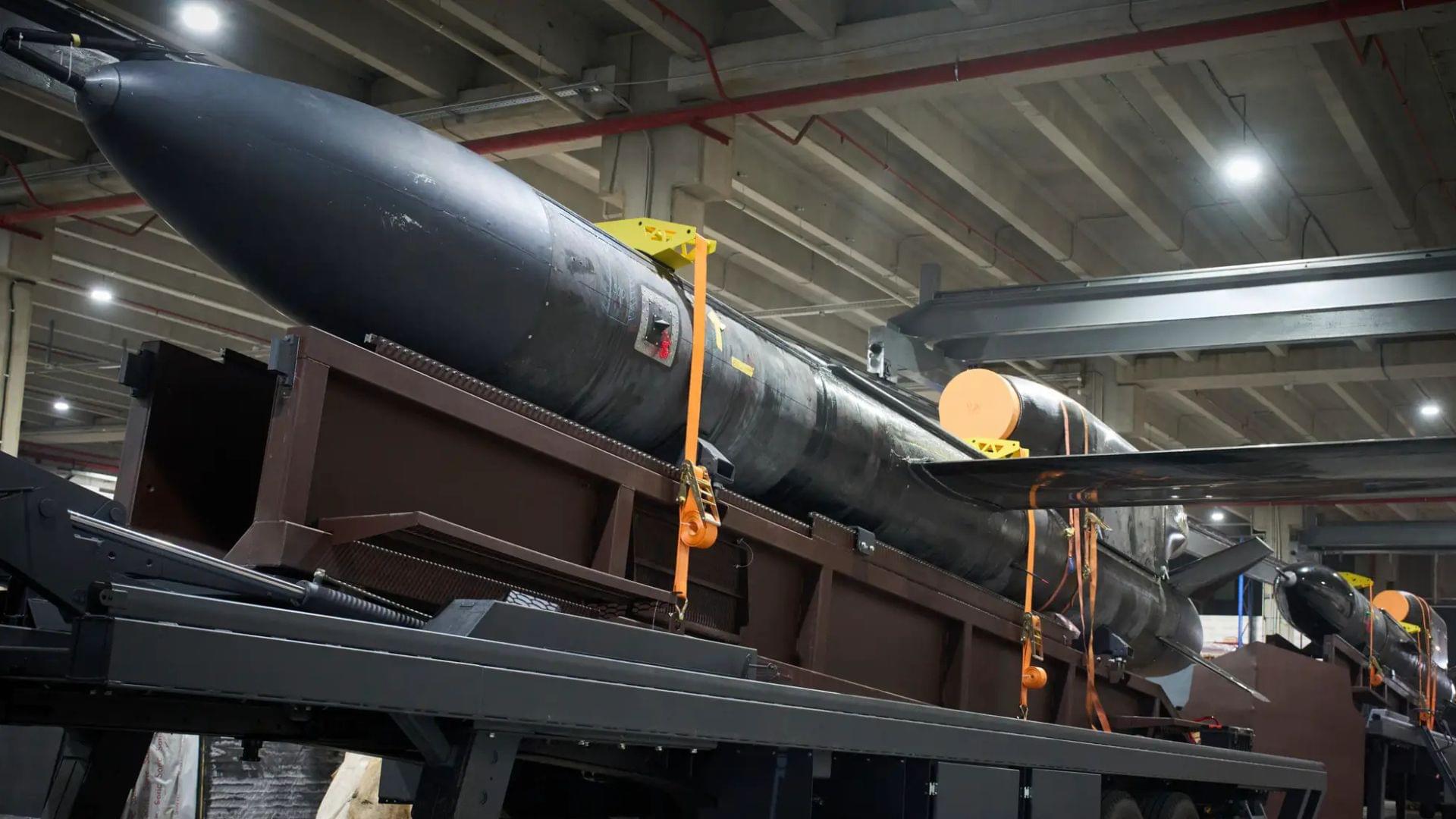
Ukraine’s biggest-ever cruise missile carries 2,205-pound warhead, 1,860-mile range.
A Ukrainian defense manufacturer has unveiled the country’s newest long-range cruise missile, the “Flamingo,” which is reportedly entering serial production, according to photographs shared on social media by an Associated Press photographer, Efrem Lukatsky, on August 18.
The images, taken inside a facility operated by the defense company Fire Point, show the missile during assembly.
According to Lukatsky, the missile is intended to strike targets more than 3,000 kilometers (1,864 miles) away, extending Ukraine’s ability to hit strategic targets deep inside Russian-controlled territory.
South Korea unveils all-muscle humanoid robot with human-level control.
Learn about ALLEX, the first general-purpose robot from WIRobotics, designed for industrial and household tasks with precision.
US startup turns cow manure into jet fuel in a move to reshape renewable energy.
Interestingly, the reactor does it all at just 1/100th the capital cost of conventional systems. The dramatic reduction in capital expenditure could make on-site fuel production a realistic prospect for individual farms.
Over 20,000 large livestock farms in the U.S. produce nearly a trillion pounds of manure annually, but less than 6% capture the biogas from this waste.
“Farmers in the U.S. and around the world are sitting on an untapped goldmine. We’re giving them the ability to turn waste into a profitable product that airlines desperately need,” said Dr. Stephen Beaton, CEO and Founder of Circularity Fuels, in the press release.


Researchers at UNIST have developed an innovative AI technology capable of reconstructing highly detailed three-dimensional (3D) models of companion animals from a single photograph, enabling realistic animations. This breakthrough allows users to experience lifelike digital avatars of their companion animals in virtual reality (VR), augmented reality (AR), and metaverse environments.