A giant new tech hub near Shanghai successfully attracted major names like Tesla, but Lingang remains almost empty of residents three years into its launch.


The Merge is the result of years of decentralized coordination and innovation. On Merge Day, ConsenSys is hosting a 72-hour mint to celebrate the achievement of Ethereum core devs, client teams and researchers. Follow the link to claim your piece of history. Links to merge.consensys-nft.com. Learn more about the NFT drop.
Quantum Computers:
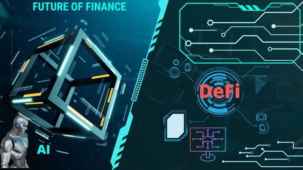
The Quantum computer is the next generation tech that works not with bits but with quantum bits (qubits) with optimized performance. Its working principle is based on the superposition i.e. Unlike the dualistic processing systems based on High and LOWs(0s), it can simultaneously be 1 and 0, or a mixture of both HIGH and LOW. Quantum computers are based on the laws of quantum mechanics to solve problems that are too complex for classical computers. Here are some key takeaways on how quantum computers assist DeFi to get boosted.
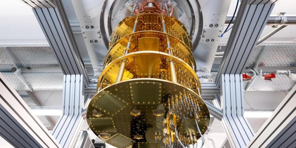
The James Webb Space Telescope has released stunning new images of the Orion nebula, a star-forming region lying about 1,300 light years away in the Orion constellation. The images are overflowing with details and are a significant improvement over the Hubble and the Spitzer images of the same. Structures down to the size of the solar system can be seen in them.
The details of the new Webb images will enable astronomers studying stellar astrophysics to understand star formation in detail. Star formation is still not fully understood, and several questions remain unanswered.
The James Webb Space Telescope has marked the beginning of a new era in astronomy. One can only imagine what the telescope will unravel in the coming years.
Sunday Discovery Series: https://bit.ly/369kG4p.
Earendel episode: https://youtu.be/-1GQIAP-o6Y
Schrodinger’s Galaxy episode: https://youtu.be/vjcuQzZD7vI
Created By: Rishabh Nakra.
Narrated By: Jeffrey Smith.
The Secrets of the Universe on the internet:
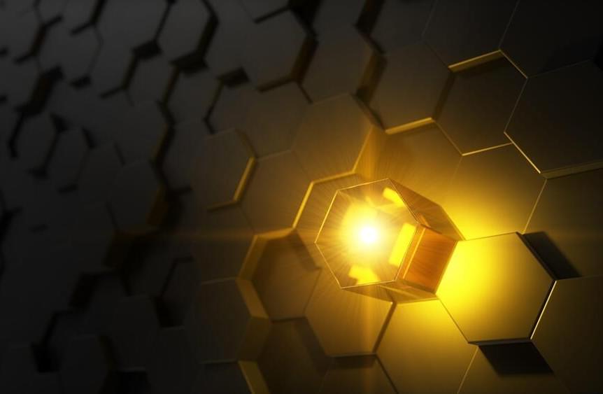
Four meteorites in northwest Africa were found to contain mysterious hexagonal diamonds that don’t naturally occur on Earth. Essentially, scientists exploring the contents of the space rocks discovered extraterrestrial materials, if you will, alien diamonds. According to Alan Salek, a member of the team that discovered the materials, “some people in the field doubted the existence of this material.” As with regular diamonds, hexagonal diamonds are made of carbon, but their atoms are arranged hexagonally rather than cubically.
The first hexagonal diamonds were recorded in meteorites in the United States and India in the 1960s and were dubbed lonsdaleite. The previously discovered crystals, however, were so small – only nanometres wide – that their hexagonality could not be confirmed. A powerful electron microscope was used by Salek and his colleagues to examine 18 meteorite samples in search of larger crystals. One of them was from Australia, and the other three were from northwestern Africa. It was found that four of the African meteorites contained hexagonal diamonds, some measuring up to a micrometer – about 1,000 times larger than anything previously discovered.
In this way, the team was able to confirm the hexagonal structure’s unusual characteristics. Salek says that now that they have larger crystals, they can get a better understanding of how they form and maybe replicate that process. Scientists are interested in Lonsdaleite since it might have even more industrial potential as a result of its theoretical hardness being stronger than a regular diamond. High-end saw blades, for instance, already contain regular diamonds.

Intellia Therapeutics said Friday the first six patients to receive its CRISPR-based treatment for a genetic swelling disorder have safely had small, corrective changes made to dysfunctional DNA inside their liver cells.
Preliminary results from the study — just the second to show that CRISPR-based gene editing can be delivered systemically and performed in vivo, or inside the body — found that the treatment, NTLA-2002, reduced levels of the disease-causing protein, kallikrein, by 65% and 92% in the low-and high-dose cohort, respectively. In the low-dose group, the one-time infusion also reduced by 91% the painful swelling “attacks” commonly experienced by patients with a rare condition called hereditary angioedema, or HAE. Participants in the high-dose group have not yet completed the 16-week observation period.
Get a Wonderful Person Tee: https://teespring.com/stores/whatdamath.
More cool designs are on Amazon: https://amzn.to/3wDGy2i.
Alternatively, PayPal donations can be sent here: http://paypal.me/whatdamath.
Hello and welcome! My name is Anton and in this video, we will talk about.
Links:
https://www.science.org/doi/10.1126/science.1060182
https://arxiv.org/pdf/1609.01639.pdf.
https://www.nsf.gov/news/mmg/mmg_disp.jsp?med_id=59577&from=
https://www.rle.mit.edu/cua_pub/ketterle_group/Projects_2001…Vortex.htm.
https://dx.doi.org/10.1103/PhysRevLett.129.061302
ISS experiments: https://youtu.be/UEEccJLYVXM
Another similar finding: https://youtu.be/FsTbMfQP7b0
#quantumphysics #blackhole #vortex.
Support this channel on Patreon to help me make this a full time job:
https://www.patreon.com/whatdamath.
Bitcoin/Ethereum to spare? Donate them here to help this channel grow!
bc1qnkl3nk0zt7w0xzrgur9pnkcduj7a3xxllcn7d4
or ETH: 0x60f088B10b03115405d313f964BeA93eF0Bd3DbF
Space Engine is available for free here: http://spaceengine.org.
Enjoy and please subscribe.
Twitter: https://twitter.com/WhatDaMath.