This is according to a report by the institution published on Tuesday.
The strongest material ever known
“For the given density, our material is the strongest known,” said Seok-Woo Lee, a materials scientist at UConn.

This is according to a report by the institution published on Tuesday.
The strongest material ever known
“For the given density, our material is the strongest known,” said Seok-Woo Lee, a materials scientist at UConn.


“O poplar tree, O poplar tree, how carbon-dense are thy branches …”
Trees are a major tool in our fight against climate change by sucking up carbon dioxide, but one company is taking them a step further: genetically engineering trees to sequester even more carbon. U.S. climate technology startup Living Carbon is developing genetically engineered seedlings of a hybrid poplar that it says can accumulate up to 53% more biomass than control plants and thereby absorb 27% more carbon.
Plants use sunlight to turn water and carbon dioxide into oxygen and sugar, a process known as photosynthesis. Living Carbon says its trees, a hybrid of the common aspen (Populus tremula) and white poplar (P. alba), can do it better with genetic changes to boost its photosynthetic performance.

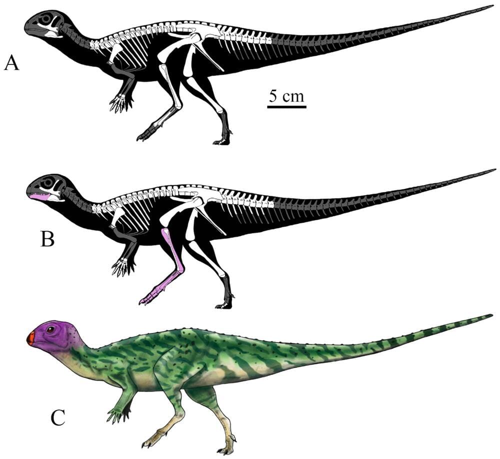
A multi-institutional team of paleontologists has identified a new dinosaur species dug up in Thailand in 2012. In their paper published in the journal Diversity, the group describes where the fossil was found, its characteristics and its condition.
The fossil was uncovered at a dig site in Phu Noi, in Northern Thailand. The geological area is known as the Phu Kradung Formation. The dig site has yielded a large number of fossils over the years. In this new effort, the research team focused their effort on a fossil embedded in stone that was in good condition. It is a previously unknown species, now named Minimocursor phunoiensis.
The research team describes the fossil as an “exceptionally articulate skeleton,” and suggest it is one the most well-preserved dinosaurs ever discovered in Southeast Asia. They found it to be of the neornithischian clade, which were plant-eating dinosaurs.

Throughout history, humans have gazed at the sky, contemplating the celestial lights, including the sun, the moon, and beyond. In those ancient moments, an insatiable curiosity ignited within them, urging them to seek answers about the origins of the cosmos. Over time, this burning curiosity has been passed down, compelling generations to develop theories in pursuit of one timeless question: Where did it all come from?
One of the most complete and widely accepted theories in this regard is the Big Bang Theory. The Big Bang is a scientific theory that proposes that the birth and development of the universe originated from a point in space-time called the singularity. Think of this in a way that all the matter and energy of the universe were trapped in an inconceivably small point of high density and high temperature (Williams & Today, n.d.). It is theorized to be a colossal release of energy that initiated the rapid expansion of the universe over 13.7 billion years that led to the creation of galaxies, stars, planetary systems and eventually humankind. What happened that led to the sudden expansion? This question continues to puzzle cosmologists, as the answer remains unknown to this day (What Is the Big Bang Theory? n.d.).
In 1915, while developing his General Theory of Relativity, Albert Einstein faced a challenge. If gravity were to solely attract all objects, the universe would ultimately collapse under its overwhelming force. However, observations indicated that the universe was not collapsing. To address this issue, Einstein introduced a cosmological constant into his equations. This constant acted as a counterforce to gravity and proposed a static model of the universe. Little did Einstein know that an astronomer named Edwin Hubble would soon contradict his proposed static model of the universe. Working at Mount Wilson Observatory in California, Hubble made a noteworthy observation in the late 1920s. He noticed a peculiar phenomenon known as redshift, where light emitted by celestial bodies moved toward the red end of the spectrum, indicating that they were moving away from us (Vogel, 2021).


Scientists have found a way to use nanotechnology to create a 3D “scaffold” to grow cells from the retina—paving the way for potential new ways of treating a common cause of blindness.
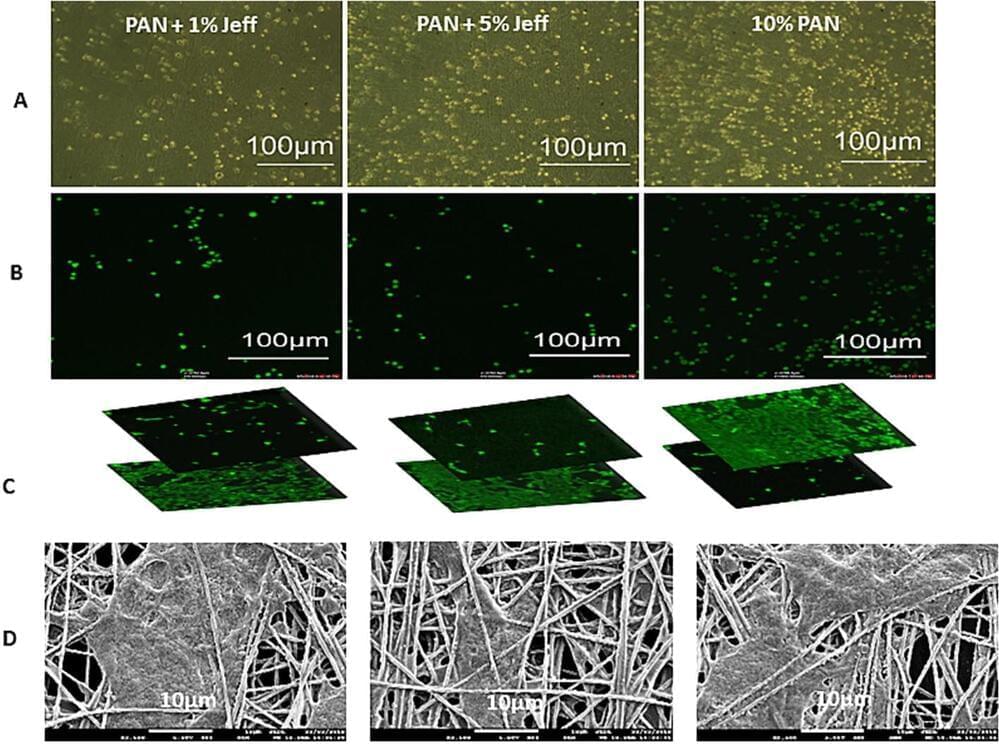
Researchers, led by Professor Barbara Pierscionek from Anglia Ruskin University (ARU), have been working on a way to successfully grow retinal pigment epithelial (RPE) cells that stay healthy and viable for up to 150 days. RPE cells sit just outside the neural part of the retina, and when damaged, can cause vision to deteriorate. Their work is published in Materials & Design.
It is the first time this technology, called “electrospinning,” has been used to create a scaffold on which the RPE cells could grow, and could revolutionize treatment for one of age-related macular degeneration, one of the world’s most common vision complaints.
The Starship upper stage’s impressive 29.5-foot diameter means it could fit up to 100 passengers at a time.
SpaceX’s Starship rocket program is the culmination of founder Elon Musk’s original plan of sending humans to Mars and making humans an interplanetary species.
And yet, Musk has always championed the launch system, originally called the Interplanetary Transport System, as a versatile spacecraft that could be used as a rapid point-to-point transportation system for Earth — a modified version of Starship has also been contracted by NASA for the Artemis III Moon landings, expected to take place in 2025.