We can’t tell much about their nature, but now we know early lifeforms included different types of organisms.



“The timing of our study couldn’t be more critical, and its implications are profound,” said Dr. Yaguang Wei.
What impact can severe air pollution have on the health of senior citizens? This is what a recent study published in BMJ hopes to address as a team of researchers led by Harvard University investigated how over-exposure to fine particulate matter (PM2.5) for senior citizens could lead to hospitalizations for seven major cardiovascular disease (CVD) subtypes, including heart failure, ischemic heart disease, arrhythmia, cerebrovascular disease, cardiomyopathy, abdominal aortic aneurysms, and thoracic aortic aneurysms. This study holds the potential to help scientists, medical professionals, and the public better understand the long-term health risks for severe air pollution, especially with climate change effects continuing to increase worldwide.
For the study, the researchers analyzed 59,761,494 Medicare fee-for-service recipients 65 years of age and older between 2000 and 2016 and compared them to air pollution data during that same period. Each of the recipients were tracked every year until their first hospitalization for one of the seven major CVD subtypes, and the researchers produced a map based on the recipients’ ZIP codes. In the end, the researchers discovered the average exposure time from air pollution to a recipients’ first hospitalization was three years, in addition to determining their exposure to PM2.5 was above the acceptable threshold outlined by the World Health Organization (WHO).

What is universal in natural languages? To answer that, deep connections need to be made between universal grammar, written codes, statistical patterns and Universal Turing machines.
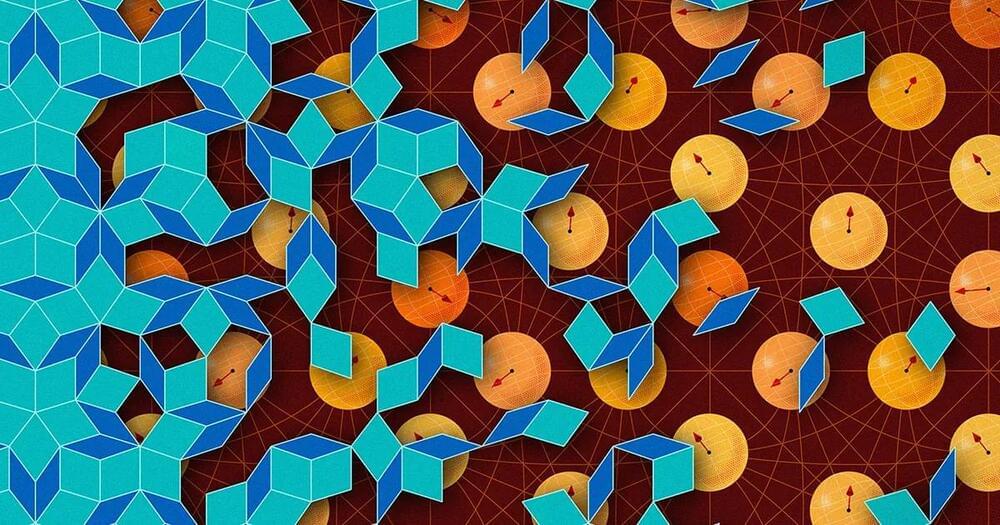
Human language is a prime example of a complex system characterized by multiple scales of description. Understanding its origins and distinctiveness has sparked investigations with very different approaches, ranging from the Universal Grammar to statistical analyses of word usage, all of which highlight, from different angles, the potential existence of universal patterns shared by all languages. Yet, a cohesive perspective remains elusive. In this paper we address this challenge. First, we provide a basic structure of universality, and define recursion as a special case thereof. We cast generative grammars of formal languages, the Universal Grammar and the Greenberg Universals in our basic structure of universality, and compare their mathematical properties. We then define universality for writing systems and show that only those using the rebus principle are universal.
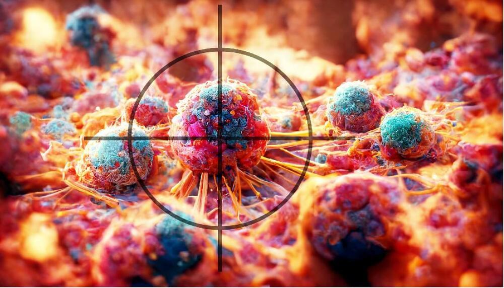
Researchers at the Technion – Israel Institute of Technology have discovered a way to potentially predict the success of immunotherapy treatment in cancer patients.
Immunotherapy involves encouraging the body’s immune system to attack the cancer cells. This can be complicated by the cancer cells “hiding” within the body or the immune system itself being reluctant to attack the cancer cells due to the threat to healthy surrounding cells.
And, while it has been proven to be a successful treatment against cancer, immunotherapy is only effective in around 40 percent of patients.


Dr. David Cohen comments on 10-year results from a trial of transcatheter vs. surgical aortic valve replacement:
Over the past decade, transcatheter aortic valve replacement (TAVR) has evolved from a niche procedure to treat severe aortic stenosis in high-risk patients to a mainstream procedure that is also performed in intermediate-and low-risk patients. With this evolution in practice, the large number of younger patients with life expectancies 10 years now receiving TAVR has raised concerns about its durability and patients’ long-term outcomes. Now, 10-year results are available from the NOTION trial of TAVR versus surgical aortic valve replacement (SAVR) that was conducted between 2009 and 2013 (NEJM JW Cardiol May 29 2015 and J Am Coll Cardiol 2015; 65:2184).
Two hundred eighty patients aged 70 years (mean age, 79 years; mean predicted risk of surgical mortality, 3%) were randomized to SAVR using any commercially available bioprosthesis or TAVR using the first-generation self-expanding CoreValve device. At 10-year follow-up, there was no significant between-group difference in the composite of death, stroke, or myocardial infarction (66% for both groups) or any of the individual components. Rates of bioprosthetic valve failure and repeat valve intervention were also similar. However, the rate of bioprosthetic valve dysfunction was lower with TAVR, largely reflecting lower rates of patient–prosthesis mismatch. The rate of structural valve deterioration was lower with TAVR as well, driven mainly by lower transvalvular gradients with TAVR that emerged early and persisted throughout follow-up.
Although limited by its modest sample size, the NOTION trial provides the longest available follow-up of any TAVR-versus-SAVR randomized trial to date. Overall, the results provide reassurance that there are no important differences in major clinical outcomes between the two strategies, and the echocardiographic data suggest sustained differences in hemodynamic performance in favor of TAVR. Nonetheless, given the advanced age of the patients at the time of enrollment, we should be cautious in extrapolating these findings to younger patients with severe aortic stenosis or to patients with bicuspid aortic valve disease (who were excluded from NOTION). These findings emphasize the tension between ongoing innovation and the desire for long-term outcomes data for our cardiac devices.
