Scientists need to learn how information flows to congressional staffers—and the crucial role they play in setting policy.

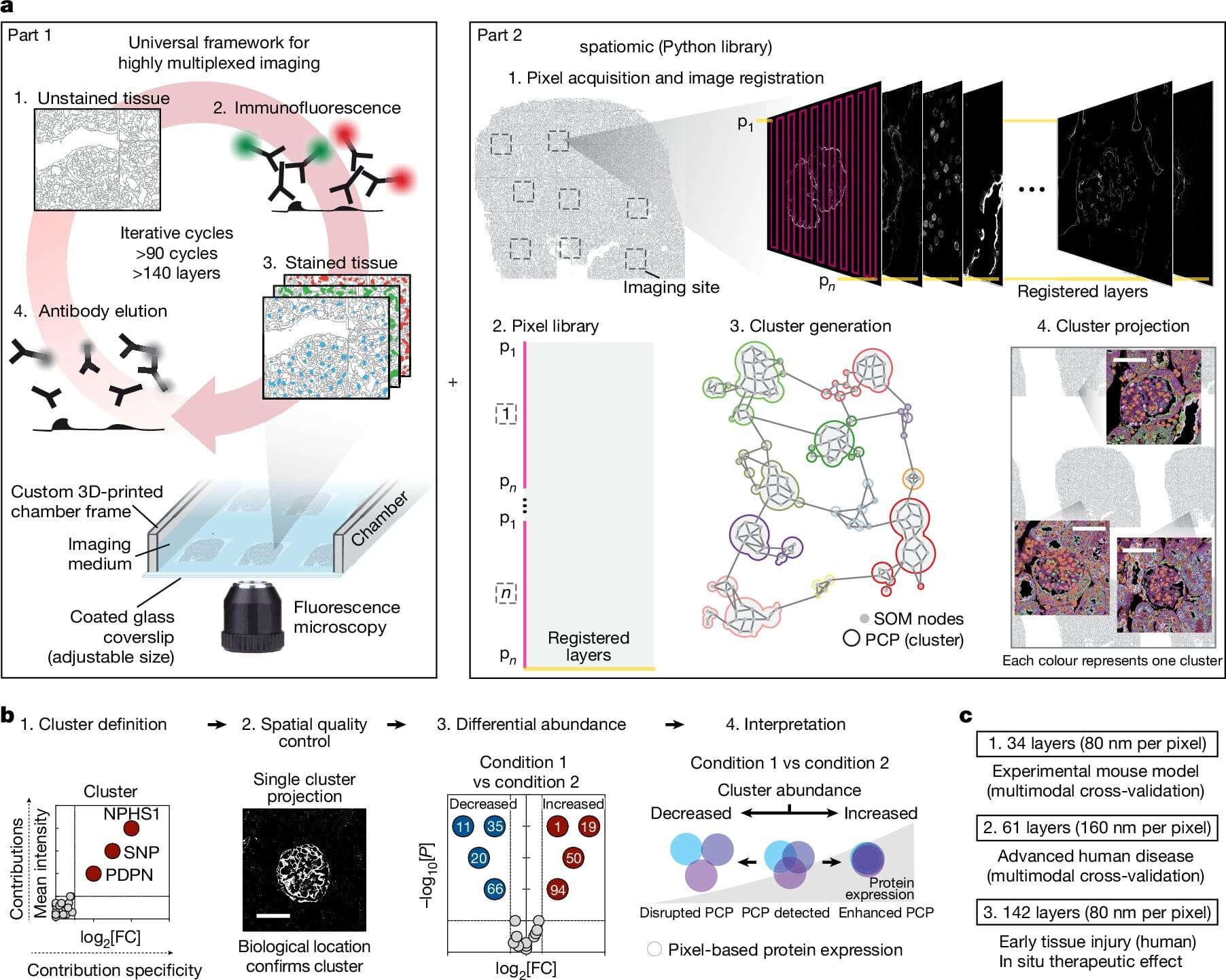
Researchers from Aarhus University—in a major international collaboration—have developed a groundbreaking method that can provide more information from the tissue samples doctors take from patients every day.
The new technique, called Pathology-oriented multiPlexing or PathoPlex, can look under a microscope at over 100 different proteins in the same small piece of tissue—instead of just 1–2 at a time, as is done now.
The technology, which has just been published in the journal Nature, combines advanced image processing with machine learning to map complex disease processes in detail.
To truly explore alien languages, linguists must open themselves to the maximum conceivable degree of cosmic otherness
Could cosmic silence be a survival strategy?
Bedrock co-founder Geoff Lewis has posted increasingly troubling content on social media, drawing concern from friends in the industry.
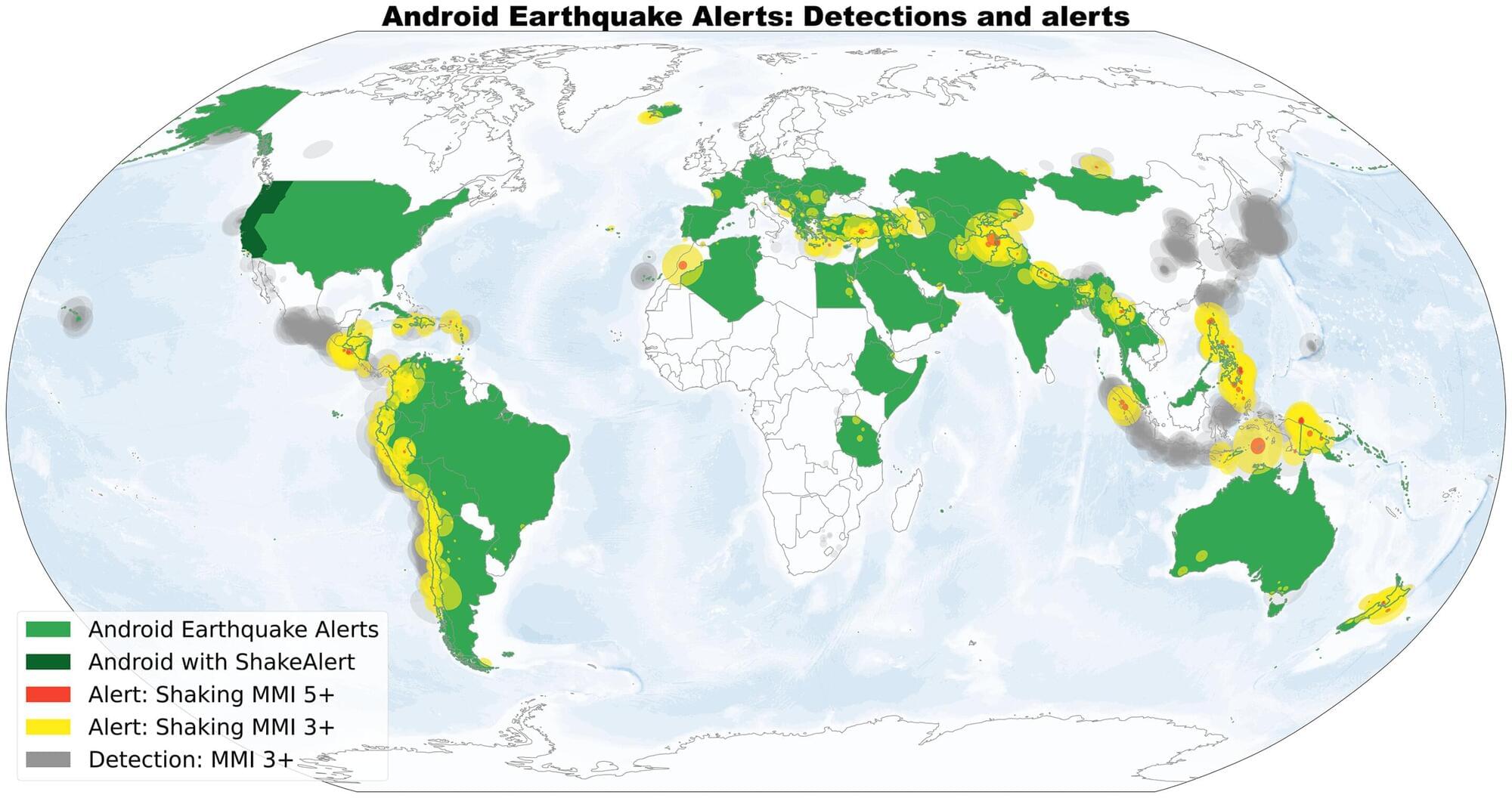
If you’re in an earthquake-prone area and own an Android phone, it could save your life. It may even have already done so. The Android Earthquake Alert (AEA) system, which began in the U.S. in 2020 and has since expanded globally, sends an automatic alert approximately one minute before the ground starts shaking. That can be enough time to take cover or warn others nearby.
In a new paper published in Science, Google explains how its detection system, which is built into most Android phones, works. They also share insights from its first years of operation and the improvements they’ve made.
Between 2021 and 2024, the AEA system sent warnings to millions of people in 98 countries. This included more than half a million people in Turkey and Syria who received an alert on February 6, 2023, just before a magnitude 7.8 earthquake struck. Overall, Google’s researchers report that alerts were issued for 1,279 events, with only three of them being false alarms, two of which were triggered by thunderstorms.

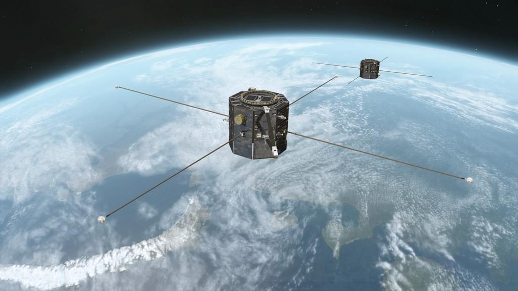
“TRACERS joins the fleet of current heliophysics missions that are actively increasing our understanding of the sun, space weather, and how to mitigate its impacts,” said Westlake.
The $170 million TRACERS is set to launch no earlier than the end of July on a SpaceX Falcon 9 rocket that will be carrying several other small missions into orbit at the same time. The answers that TRACERS could provide about how magnetic reconnection works will allow scientists to better protect critical infrastructure for when solar storms hit.
“It’s going to help us keep our way of life safe here on Earth,” said Westlake.