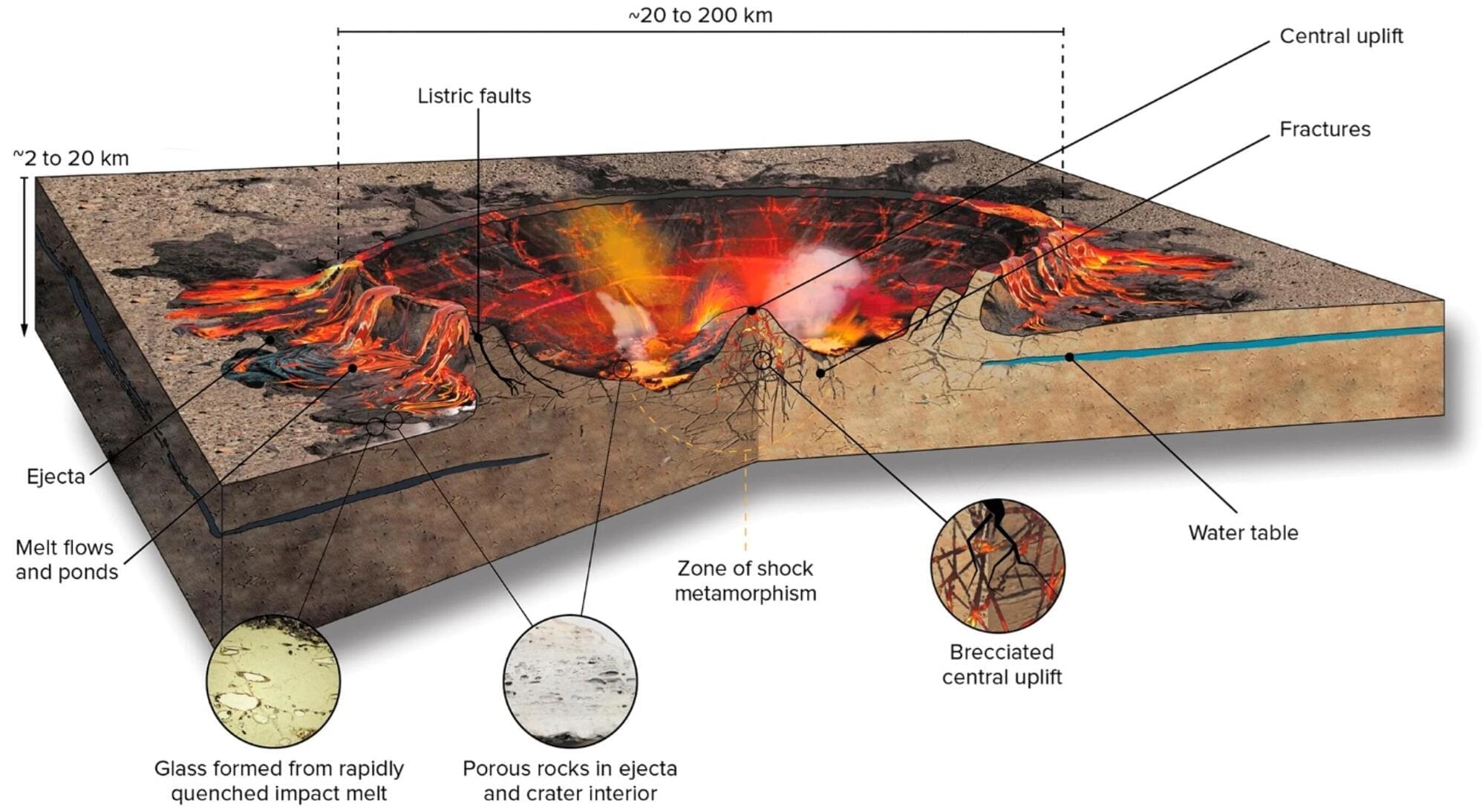
Meteor impacts may have helped spark life on Earth, creating hot, chemical-rich environments where the first living cells could take shape, according to research integrated by a recent Rutgers University graduate. Shea Cinquemani, who earned her bachelor’s degree from the School of Environmental and Biological Sciences in May 2025, has published a paper based on research she started during the spring of her senior year.
“No one knows, from a scientific perspective, how life could have been formed from an early Earth that had no life,” said Shea Cinquemani, who earned her bachelor’s degree in marine biology and fisheries management from the Rutgers School of Environmental and Biological Sciences in May 2025. “How does something come from nothing?”
Cinquemani is the lead author of a review, published in the Journal of Marine Science and Engineering, examining where life may have first formed on Earth. The paper focuses on hydrothermal vents, places where hot, mineral-rich water flows through rock and emerges into surrounding water, creating the chemical conditions and energy gradients needed for complex reactions.