Toggle light / dark theme

Ferroelectrics at the nanoscale exhibit a wealth of polar and sometimes swirling (chiral) electromagnetic textures that not only represent fascinating physics, but also promise applications in future nanoelectronics. For example, ultra-high-density data storage or extremely energy-efficient field-effect transistors. However, a sticking point has been the stability of these topological textures and how they can be controlled and steered by an external electrical or optical stimulus.

A team led by Prof. Catherine Dubourdieu (HZB and FU Berlin) has now published a paper in Nature Communications that opens up new perspectives. Together with partners from the CEMES-CNRS in Toulouse, the University of Picardie in Amiens and the Jozef Stefan Institute in Ljubljana, they have thoroughly investigated a particularly interesting class of nanoislands on silicon and explored their suitability for electrical manipulation.

“We have produced BaTiO3 nanostructures that form tiny islands on a silicon substrate,” explains Dubourdieu. The nano-islands are trapezoidal in shape, with dimensions of 30–60 nm (on top), and have stable polarization domains.

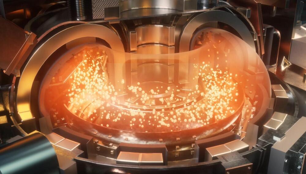
In a pioneering approach to achieve fusion energy, the SMART device has successfully generated its first tokamak plasma. This step brings the international fusion community closer to achieving sustainable, clean, and virtually limitless energy through controlled fusion reactions.

The work is published in the journal Nuclear Fusion.

The SMART tokamak, a state-of-the-art experimental fusion device designed, constructed and operated by the Plasma Science and Fusion Technology Laboratory of the University of Seville, is a unique spherical tokamak due to its flexible shaping capabilities. SMART has been designed to demonstrate the unique physics and engineering properties of Negative Triangularity shaped plasmas towards compact fusion power plants based on Spherical Tokamaks.

University of Missouri scientists are unlocking the secrets of halide perovskites—a material that’s poised to reshape our future by bringing us closer to a new age of energy-efficient optoelectronics.

Suchi Guha and Gavin King, two physics professors in Mizzou’s College of Arts and Science, are studying the material at the nanoscale: a place where objects are invisible to the naked eye. At this level, the extraordinary properties of halide perovskites come to life, thanks to the material’s unique structure of ultra-thin crystals—making it astonishingly efficient at converting sunlight into energy.

Think that are not only more affordable but also far more effective at powering homes. Or LED lights that burn brighter and last longer while consuming less energy.

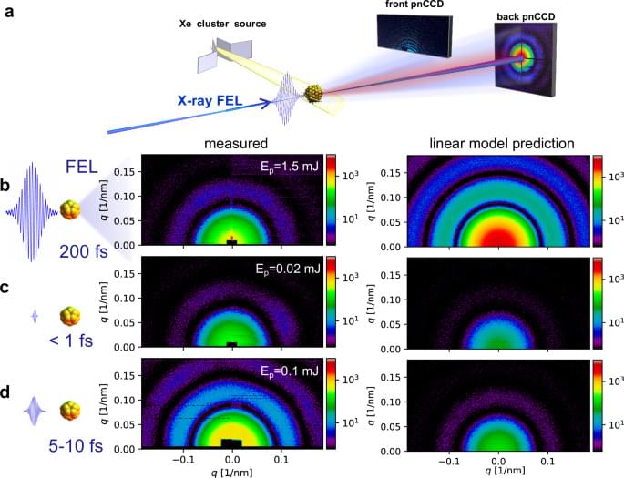
Diffraction-before-destruction of ultrashort X-ray pulses can visualize non-equilibrium processes at the nanoscale with sub-femtosecond precision. Here, the authors demonstrate how the brightness and the spatial resolution of such snapshots can be substantially increased despite ionization.

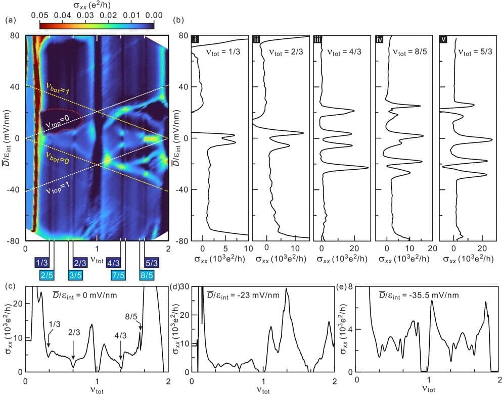
A research team discovered a quantum state in which electrons move in a completely new way under a twisted graphene structure. The unique electronic state is expected to contribute to the development of more efficient and faster electronic devices. It may also be applicable to technologies such as quantum memory, which can process complex computations.

Quantum physics is a crucial theory that attempts to understand and explain how atoms and particles interact and move in nature. Such an understanding serves as the basis for designing new technologies that control or utilize nature at the microscopic level. The research conducted holds significance in discovering the , which is difficult to implement with conventional semiconductor technologies, and in greatly expanding future possibilities for quantum technologies.

Graphene is a material as thin as a piece of paper and is made of carbon atoms. This study utilized a unique structure comprising two slightly twisted layers of graphene, observing a new quantum state. When compared to two transparent films, each film has regular patterns, and when they are rotated slightly, the patterns overlap to reveal new patterns.

The Experimental Advanced Superconducting Tokamak (EAST), commonly known as China’s “artificial sun,” has achieved a remarkable scientific milestone by maintaining steady-state high-confinement plasma operation for an impressive 1,066 seconds. This accomplishment, reached on Monday, sets a new world record and marks a significant breakthrough in the pursuit of fusion power generation.

The duration of 1,066 seconds is a critical advancement in fusion research. This milestone, achieved by the Institute of Plasma Physics (ASIPP) at Hefei Institutes of Physical Science (HFIPS) of the Chinese Academy of Sciences, far surpasses the previous world record of 403 seconds, also set by EAST in 2023.

The ultimate goal of developing an artificial sun is to replicate the nuclear fusion processes that occur in the sun, providing humanity with a limitless and clean energy source, and enabling exploration beyond our solar system.

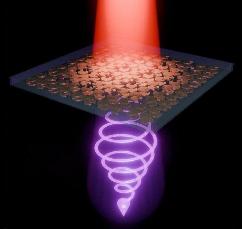
Researchers have developed a revolutionary ultra-thin metasurface that can generate circularly polarized light with remarkable efficiency.

By leveraging the unique properties of chirality and rotational symmetry, this breakthrough eliminates the need for bulky optical setups, enabling more compact and efficient optical devices. This innovation has far-reaching implications for fields such as medical imaging, communications, and quantum physics.

Advancing Optical Technology with Metasurfaces.

Microdrop Technologies is the leading provider of dispensing equipment, software and services for advanced microdispensing and inkjet printing applications.

Our team of scientists, engineers and technicians has more than 30 years of experiences in inkjet-technology and microfluidics. We focus on high quality products and services for Life Science and industrial applications as well as R&D purposes. For the best benefit, we provide our customers a number of services. microdrop is in involved in several R&D projects with industrial partners or by public funding.

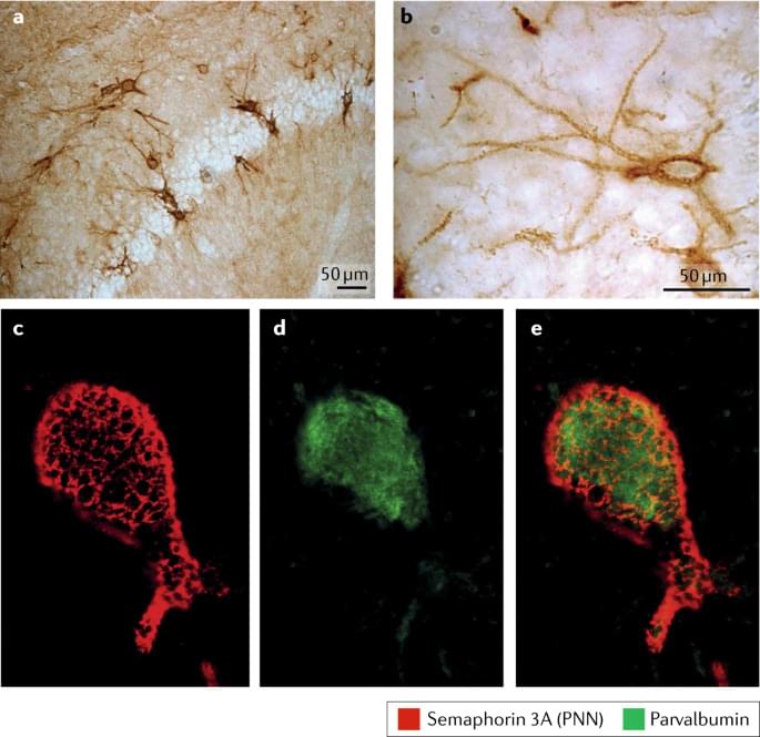
Specialized extracellular matrix structures known as perineuronal nets surround the soma and dendrites of many CNS neurons. Fawcett and colleagues provide an update on our current understanding of perineuronal net composition, formation and functional roles in brain function and disease.

The Stargate Project is a new company which intends to invest $500 billion over the next four years building new AI infrastructure for OpenAI in the United States. We will begin deploying $100 billion immediately. This infrastructure will secure American leadership in AI, create hundreds of thousands of American jobs, and generate massive economic benefit for the entire world. This project will not only support the re-industrialization of the United States but also provide a strategic capability to protect the national security of America and its allies.

The initial equity funders in Stargate are SoftBank, OpenAI, Oracle, and MGX. SoftBank and OpenAI are the lead partners for Stargate, with SoftBank having financial responsibility and OpenAI having operational responsibility. Masayoshi Son will be the chairman.

Arm, Microsoft, NVIDIA, Oracle, and OpenAI are the key initial technology partners. The buildout is currently underway, starting in Texas, and we are evaluating potential sites across the country for more campuses as we finalize definitive agreements.