There are only four super star clusters in all the Local Group: rarities today. Here’s what the youngest, the just-discovered N79, shows us.
Get the latest international news and world events from around the world.

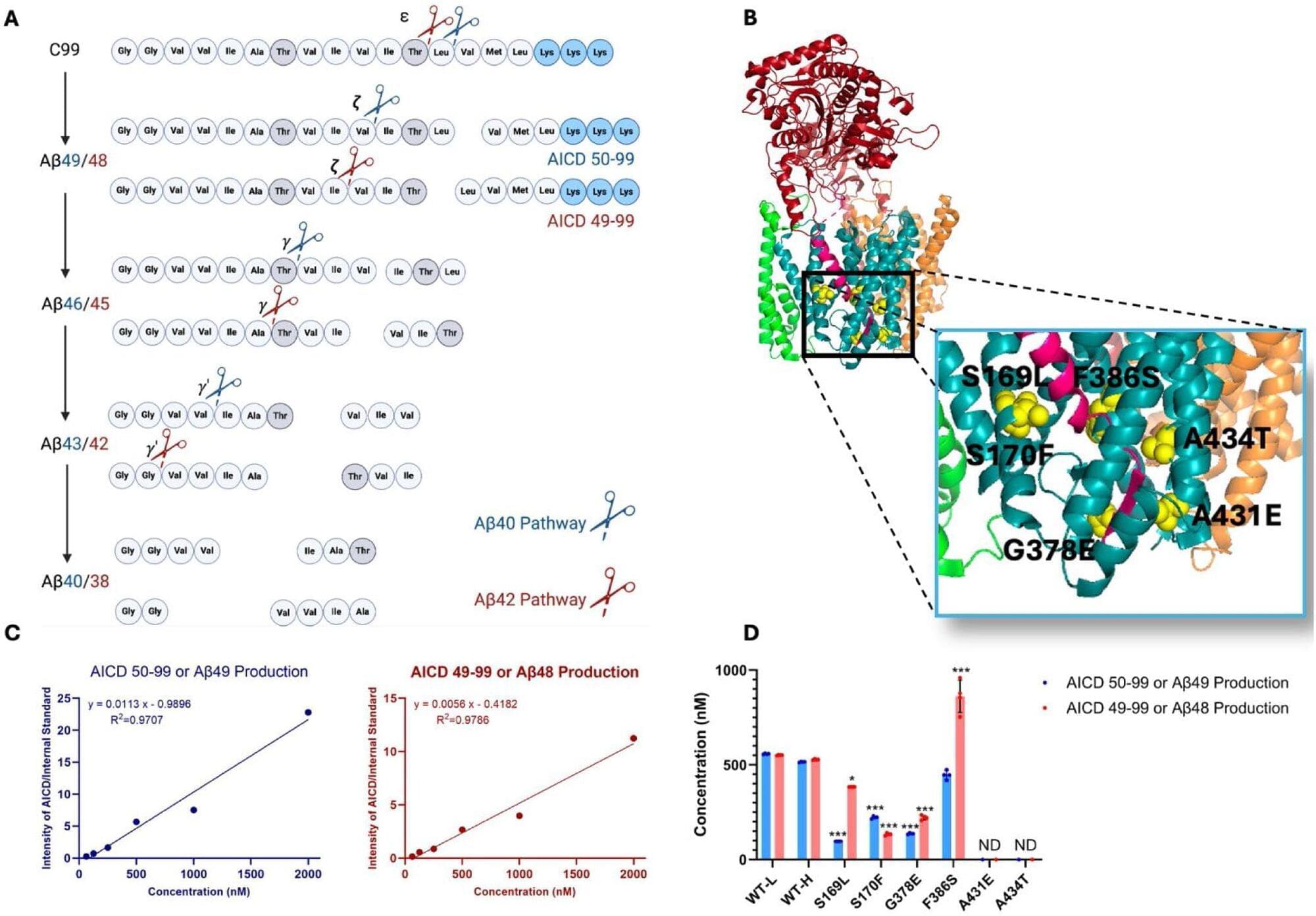
A disrupted protein recycling process can harm heart health
A disrupted protein degradation process in heart muscle cells can lead to a range of severe heart diseases. In the case of dilated cardiomyopathy, a pathological enlargement of the heart chambers, researchers at the Max Planck Institute for Heart and Lung Research in Bad Nauheim have now identified a cause: a low level of the enzyme Ubiquitin-specific peptidase 5 (USP5) leads to an accumulation of Ubiquitin in heart muscle cells and the formation of protein aggregates, which trigger heart diseases. Increasing USP5 levels in heart muscle cells protects the heart from harmful degradation processes, offering a perspective for new therapies.
Dilated cardiomyopathy is a pathological enlargement of one or both heart chambers, including the atria. The resulting restriction of heart function is caused by structural damage to heart muscle cells. The consequence is heart failure, which can lead to death without a heart transplant. Existing therapeutic options can usually not stop or reverse the progression of the disease.
In search of new therapeutic approaches, researchers from the department of Thomas Braun at the Max Planck Institute for Heart and Lung Research have investigated the molecular processes of protein degradation in heart muscle cells. Yvonne Eibach and Silke Kreher, both first authors of the study published in Science Advances, together with their research partners, discovered disturbances in the process that serves the disposal of defective or no longer needed proteins.
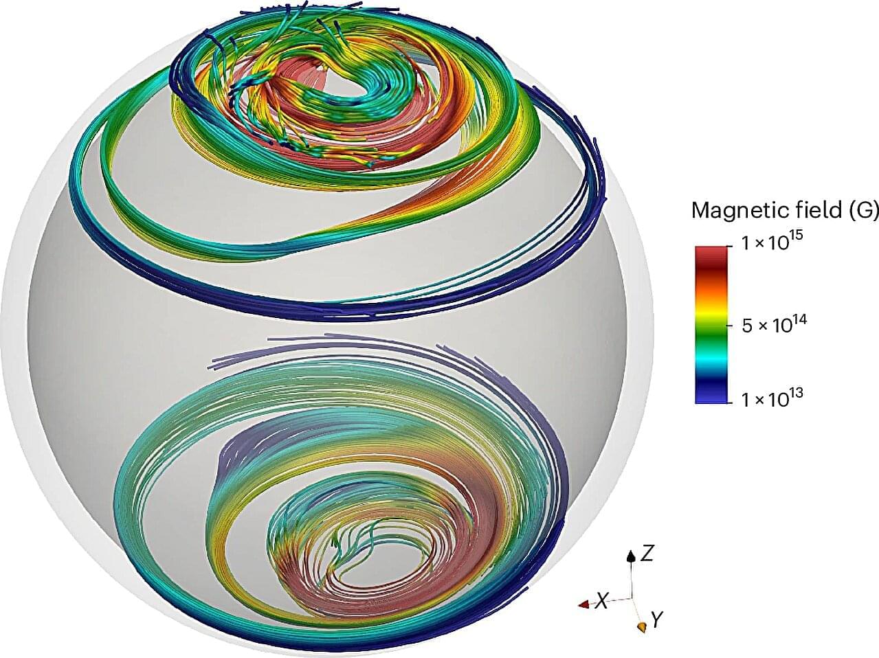
Model shows spinning neutron stars gain enormous magnetic fields
An international team of scientists has modeled the formation and evolution of the strongest magnetic fields in the universe.
Led by scientists from Newcastle University, University of Leeds and France, the paper was published in the journal Nature Astronomy. The researchers identified the Tayler-Spruit dynamo caused by the fall back of supernova material as a mechanism leading to the formation of low-field magnetars. This new work solves the mystery of low-field magnetar formation, which has puzzled scientists since low-field magnetar discovery in 2010.
The team used advanced numerical simulations to model the magneto-thermal evolution of these stars, finding that a specific dynamo process within the proto-neutron star can generate these weaker magnetic fields.

The 100-year-old symmetry theorem that is still changing physics today
Emmy Noether was hailed as a mathematical genius in her own time. And her theorem on symmetry is still driving new discoveries in particle physics and quantum computing today.
By John Gribbin and Mary Gribbin.

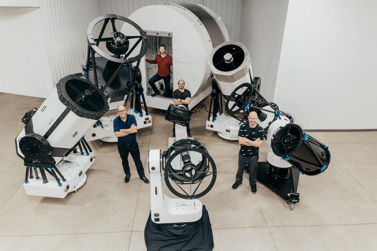
Two space startups have merged to create the next generation of telescopes
On a clear spring evening in Michigan, the stars aligned — just not in the way Upfront Ventures partner Nick Kim expected.
He’d just led a $9.5 million seed round for OurSky, a software platform for space observational data, and was eager to see what its telescope partner PlaneWave Instruments could do.
But when they rolled out the telescopes that night at PlaneWave’s manufacturing facility, he was stuck waiting.

Taking omega-3 supplements may slow down aging, a new study finds
An international team of scientists, including researchers from Harvard University and the University of Zurich, analyzed clinical trial results 777 elderly Swiss adults to test the potential anti-aging benefits of supplements and exercise.
While there’s no perfect way to measure biological aging, the researchers used tools that help measure age-related decline in the cells and organs, including factors like brain health and heart health.
They looked at participants who underwent one of eight longevity treatments over three years, including exercising and supplementing omega-3s, vitamin D, or both.

Magnetic Fields Reshape the Movement of Sound Waves in a Stunning Discovery
The term “nanoscale” refers to dimensions that are measured in nanometers (nm), with one nanometer equaling one-billionth of a meter. This scale encompasses sizes from approximately 1 to 100 nanometers, where unique physical, chemical, and biological properties emerge that are not present in bulk materials. At the nanoscale, materials exhibit phenomena such as quantum effects and increased surface area to volume ratios, which can significantly alter their optical, electrical, and magnetic behaviors. These characteristics make nanoscale materials highly valuable for a wide range of applications, including electronics, medicine, and materials science.
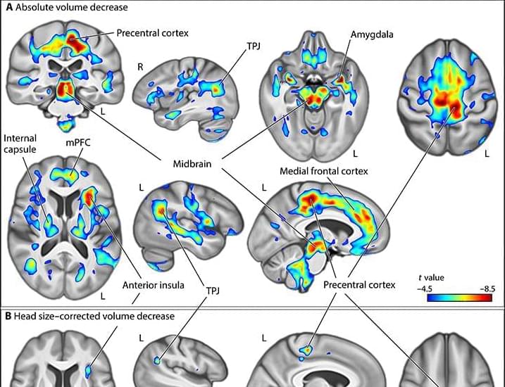
Distinct impact modes of polygenic disposition to dyslexia in the adult brain
A recent large-scale study published in Science Advances has revealed a connection between genetic variations associated with dyslexia and structural differences in the brain. These differences were found in areas involved in motor coordination, vision, and language. This provides new insights into the neurological underpinnings of this common learning difficulty.
Dyslexia is a common learning difficulty that primarily affects the skills involved in accurate and fluent word reading and spelling. It’s characterized by challenges with phonological awareness (the ability to recognize and manipulate the sounds in spoken language), verbal memory, and verbal processing speed. People with dyslexia may struggle to decode words, recognize familiar words automatically, and spell words correctly. Importantly, dyslexia is not related to a person’s overall intelligence. It’s considered a neurodevelopmental condition, meaning it arises from differences in how the brain develops and processes information, particularly related to language.
Genetic disposition to dyslexia is associated with brain structure in the general population.