Deep inside the electronic devices that proliferate in our world, from cell phones to solar cells, layer upon layer of almost unimaginably small transistors and delicate circuitry shuttle all-important electrons back and forth.
It is now possible to cram 6 million or more transistors into a single layer of these chips. Designers include layers of glassy materials between the electronics to insulate and protect these delicate components against the continual push and pull of heating and cooling that often causes them to fail.
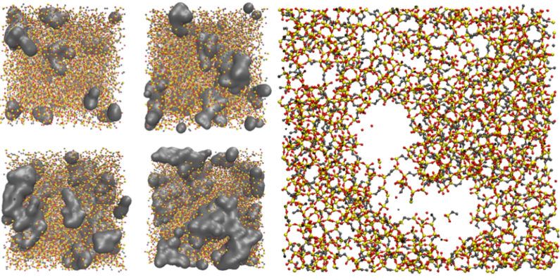
A paper published today in the journal Nature Materials reshapes our understanding of the materials in those important protective layers. In the study, Stanford’s Reinhold Dauskardt, a professor of materials science and engineering, and doctoral candidate Joseph Burg reveal that those glassy materials respond very differently to compression than they do to the tension of bending and stretching. The findings overturn conventional understanding and could have a lasting impact on the structure and reliability of the myriad devices that people depend upon every day.


 © iStock/ Getty Images undefined How much storage do you have around the house? A few terabyte hard drives? What about USB sticks and old SATA drives? Humanity uses a staggering amount of storage, and our needs are only expanding as we build data centers, better cameras, and all sorts of other data-heavy gizmos. It’s a problem scientists from companies like IBM, Intel, and Microsoft are trying to solve, and the solution might be in our DNA.