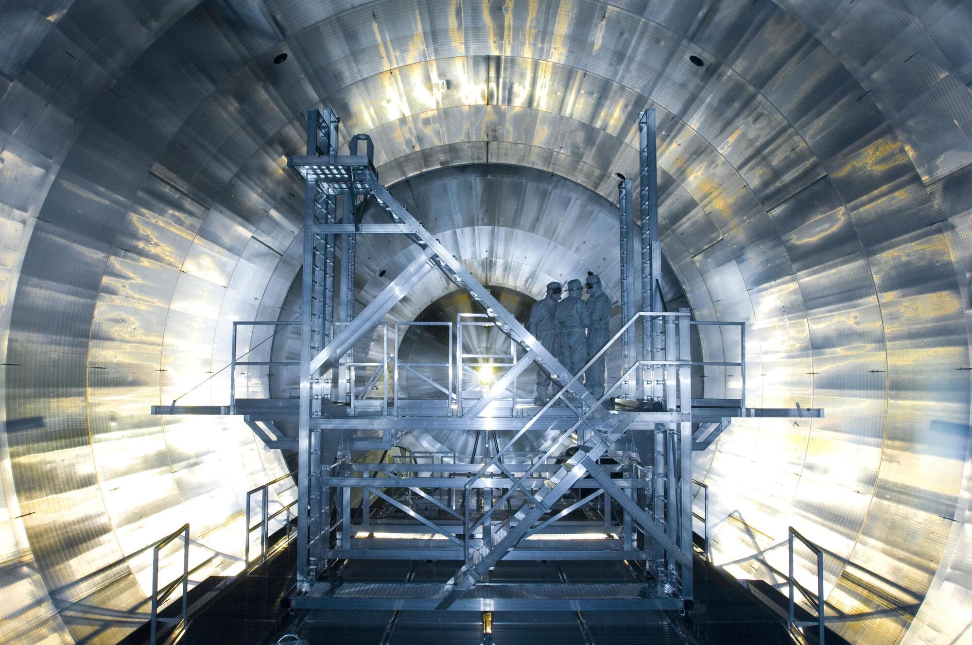
Toggle light / dark theme

Microscopic chinks in material just several atoms thick have the potential to advance a multitude of quantum technologies, new research shows – getting us closer to the widespread use of quantum networks and sensors.

Right now, storing quantum data in the spin properties of electrons, known as spin coherence, requires a very particular and delicate laboratory setup. It’s not something you can do without a carefully controlled environment.

Here, an international team of researchers managed to demonstrate observable spin coherence at room temperature, using the tiny defects in a layered 2D material called Hexagonal Boron Nitride (hBN).

Group theory and first-principles calculations combine to predict which antiferromagnets have potentially useful net surface magnetization.

Antiferromagnetism was discovered in the 1930s by Louis Néel but had long been considered of scientific, not practical, interest. Antiferromagnets (AFM) are internally magnetic, but the magnetic moments of their atoms and molecules are antiparallel to each other, canceling out and resulting in no net magnetization. This cancellation renders bulk antiferromagnets effectively invisible to external magnetic fields, so that their magnetic properties are difficult to harness in applications. Recently, however, a new paradigm has appeared—antiferromagnetism-based spintronics—which seeks to apply antiferromagnets’ unique properties (such as fast spin dynamics, the absence of strong stray fields, and the stability of these materials) to the processing and storage of information [1].

Materials scientists and engineers would like to know precisely how electrons interact and move in new materials and how the devices made with them will behave. Will the electrical current flow easily within the material? Is there a temperature at which the material will become superconducting, enabling current to flow without a power source? How long will the quantum state of an electron spin be preserved in new electronic and quantum devices?

Lying between the microwave and infrared regions of the electromagnetic spectrum, the terahertz (1 THz = 10¹² Hz) gap is being rapidly closed by development of new terahertz sources and detectors, with promising applications in spectroscopy, imaging, sensing, and communication.

These applications greatly benefit from terahertz sources delivering high-energy or high-average-power radiation. On the other hand, high-intensity or strong-field terahertz sources are essential to observe or exploit novel nonlinear terahertz-matter interactions, where the electric and/or magnetic field strengths play a key role.

The team of scientists, led by Dr. Chul Kang from Advanced Photonics Research Institute, Gwangju Institute of Science and Technology (GIST), Korea, and Professor Ki-Yong Kim from Institute for Research in Electronics and Applied Physics, University of Maryland, College Park, Maryland, U.S., has created the world’s strongest terahertz fields of 260 megavolts per centimeter (MV/cm) or equivalent peak intensity of 9 × 10¹³ watts per square centimeter (W/cm²).