Page 10845
Feb 29, 2016
Graphene Patterned After Moth Eyes Could Give Us ‘Smart Wallpaper’
Posted by Shailesh Prasad in category: materials
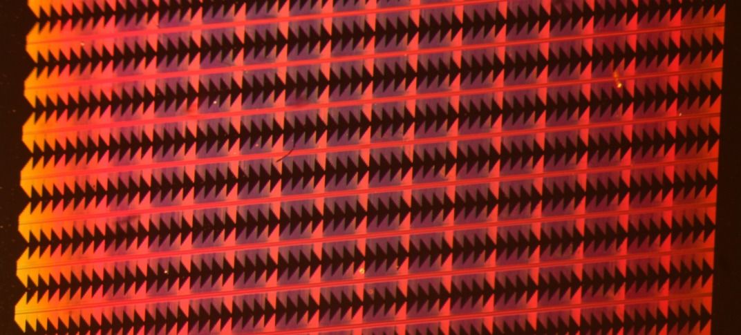
Tweaking the structure of graphene so that it matches patterns found in the eyes of moths could one day give us “smart wallpaper,” among a host of other useful technologies.
Using a novel technique called “nano texturing,” scientists at the University of Surrey in England have successfully modified ultra-thin graphene sheets to create the most efficient light-absorbent material to date, which is capable of generating electricity from both captured light and waste heat. They described their work in a new paper in Science Advances.
Continue reading “Graphene Patterned After Moth Eyes Could Give Us ‘Smart Wallpaper’” »
Feb 29, 2016
Want to avoid breaches Think like a hacker
Posted by Karen Hurst in category: cybercrime/malcode

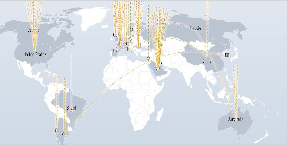
One philosophy that I have often practice and encourage my team to do is to think like a hacker. It has served me and my teams well. At times; I have shared areas where risks exist in the emerging technologies; and hope that I don’t make folks too nervous. However, we all have to start thinking like hackers or pay the cost some day.
C-level executives from giant corporations and officials from the smallest companies all must think like hackers and test their cyber defenses regularly if they expect to avoid breaches of their systems.
That’s according to a panel of cybersecurity experts who recently spoke to a crowd gathered at the Donald Danforth Plant Science Center.
Continue reading “Want to avoid breaches Think like a hacker” »
Feb 29, 2016
Imaging algorithm gathers information about how cells move
Posted by Shailesh Prasad in categories: biotech/medical, information science
Brown University engineers have developed a new technique to help researchers understand how cells move through complex tissues in the body. They hope the tool will be useful in understanding all kinds of cell movements, from how cancer cells migrate to how immune cells make their way to infection sites.
The technique is described in a paper published in the Proceedings of the National Academy of Sciences.
The traditional method for studying cell movement is called traction force microscopy (TFM). Scientists take images of cells as they move along 2-D surfaces or through 3-D gels that are designed as stand-ins for actual body tissue. By measuring the extent to which cells displace the 2-D surface or the 3-D gel as they move, researchers can calculate the forces generated by the cell. The problem is that in order to do the calculations, the stiffness and other mechanical properties of artificial tissue environment must be known.
Read more
Feb 29, 2016
How modern technology could have solved every problem in literary history
Posted by Shailesh Prasad in category: mobile phones

Feb 29, 2016
America’s Space Heritage Is Rotting ‘In Place’
Posted by Bruce Dorminey in category: space

New book chronicles American space history left rotting at the pad; not just at Cape Canaveral but across the U.S. Not sure what can be done with behemoth launch pads, but perhaps a non-profit effort at restoring them or at least cleaning them up might be worth the effort.
Large swaths of America’s space heritage have literally been left to rot at the launch pad as is poignantly made clear in Abandoned In Place, a new book that chronicles long-neglected and largely forgotten aspects of U.S. space history.
Author Roland Miller’s oversized collection of photos and essays documents some 60 years of U.S. space history mostly at Cape Canaveral, Fla.
Continue reading “America’s Space Heritage Is Rotting ‘In Place’” »
Feb 29, 2016
Physicists promise a copper revolution in nanophotonics
Posted by Shailesh Prasad in categories: computing, electronics, nanotechnology, physics
Researchers from the Moscow Institute of Physics and Technology (MIPT) have for the first time experimentally demonstrated that copper nanophotonic components can operate successfully in photonic devices – it was previously believed that only gold and silver components could do so. Copper components are not only just as good as components based on noble metals; they can also be easily implemented in integrated circuits using industry-standard fabrication processes. “This is a kind of revolution – using copper will solve one of the main problems in nanophotonics,” say the authors of the paper. The results have been published in the scientific journal Nano Letters.
The discovery, which is revolutionary for photonics and the computers of the future, was made by researchers from the Laboratory of Nanooptics and Plasmonics at MIPT’s Centre of Nanoscale Optoelectronics. They have succeeded, for the first time, in producing copper nanophotonic components, whose characteristics are just as good as those of gold components. It is interesting to note that the scientists fabricated the copper components using the process compatible with the industry-standard manufacturing technologies that are used today to produce modern integrated circuits. This means that in the very near future copper nanophotonic components will form a basis for the development of energy-efficient light sources, ultra-sensitive sensors, as well as high-performance optoelectronic processors with several thousand cores.
The discovery was made under what is known as nanophotonics – a branch of research which aims, among other things, to replace existing components in data processing devices with more modern components by using photons instead of electrons. However, while transistors can be scaled down in size to a few nanometres, the diffraction of light limits the minimum dimensions of photonic components to the size of about the light wavelength (~1 micrometre). Despite the fundamental nature of this so-called diffraction limit, one can overcome it by using metal-dielectric structures to create truly nanoscale photonic components. Firstly, most metals show a negative permittivity at optical frequencies, and light cannot propagate through them, penetrating to a depth of only 25 nanometres. Secondly, light may be converted into surface plasmon polaritons, surface waves propagating along the surface of a metal. This makes it possible to switch from conventional 3D photonics to 2D surface plasmon photonics, which is known as plasmonics. This offers the possibility of controlling light at a scale of around 100 nanometres, i.e., far beyond the diffraction limit.
Continue reading “Physicists promise a copper revolution in nanophotonics” »
Feb 29, 2016
A Material That’s Better Than Graphene? Scientists Say They’ve Found it
Posted by Shailesh Prasad in categories: materials, particle physics
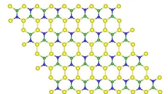
What could be better than a material that’s super flexible, only one atom thick, and is 200 times stronger than steel? A material that’s equally strong and flexible, also only one atom thick, and inexpensive.
Scientists are asserting that this new discovery could potentially upstage the world’s greatest wonder material, graphene.
Read more