New details were shared months after a home exploded in Leland, North Carolina earlier this year.


IN A NUTSHELL 🚁 The Cavorite X7 is the world’s first ‘heli-plane’, offering a revolutionary blend of helicopter and airplane capabilities. 🌟 Featuring a fan-in-wing design, it achieves vertical takeoff and transitions to high-speed flight seamlessly. 📦 With a cargo capacity of up to 1,500 lbs, it serves as an efficient solution for both passenger

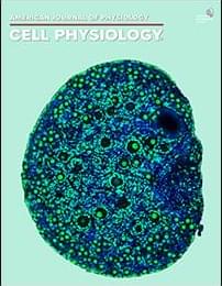
Bioactive phytochemicals, phenolic compounds, terpenoids, and alkaloids, exert antioxidative, anti-inflammatory, antigenotoxic, and anticancer effects, simultaneously showing minimal or no toxicity on normal, healthy cells. Phytochemicals targeting various signaling pathways and multiple mechanisms underlying intrinsic and acquired multidrug resistance (MDR) in cancer cells make them invaluable tools for the development of novel strategies for fighting against anticancer drug resistance in different types of cancer, which is one of the ultimate goals of modern oncology research. As MDR is described to be a simultaneous development of resistance to multiple drugs with different chemical structures, mechanisms of action, and targets it is not surprising that multiple factors, such as genetic and epigenetic changes, as well as noncoding RNAs, including microRNAs may significantly contribute to the development MDR in cancer cells, and its targeting and modulation of their expression to sensitize cells to treatment. This review implies that some natural compounds, such as curcumin, resveratrol, kaempferol, allicin, and quercetin, have the potential to interact with highly oncogenic and/or proinflammatory miRNAs, such as miR-21/155/663/146a, significantly influencing the response to cancer therapy. This article aims to point out how natural compounds may be used, accompanied by miRNAs mimics or miRNA inhibitors to treat specific types of cancer and its subtypes to overcome multidrug resistance. The main challenge is to determine the proper doses and concentrations of both miRNAs and compounds.
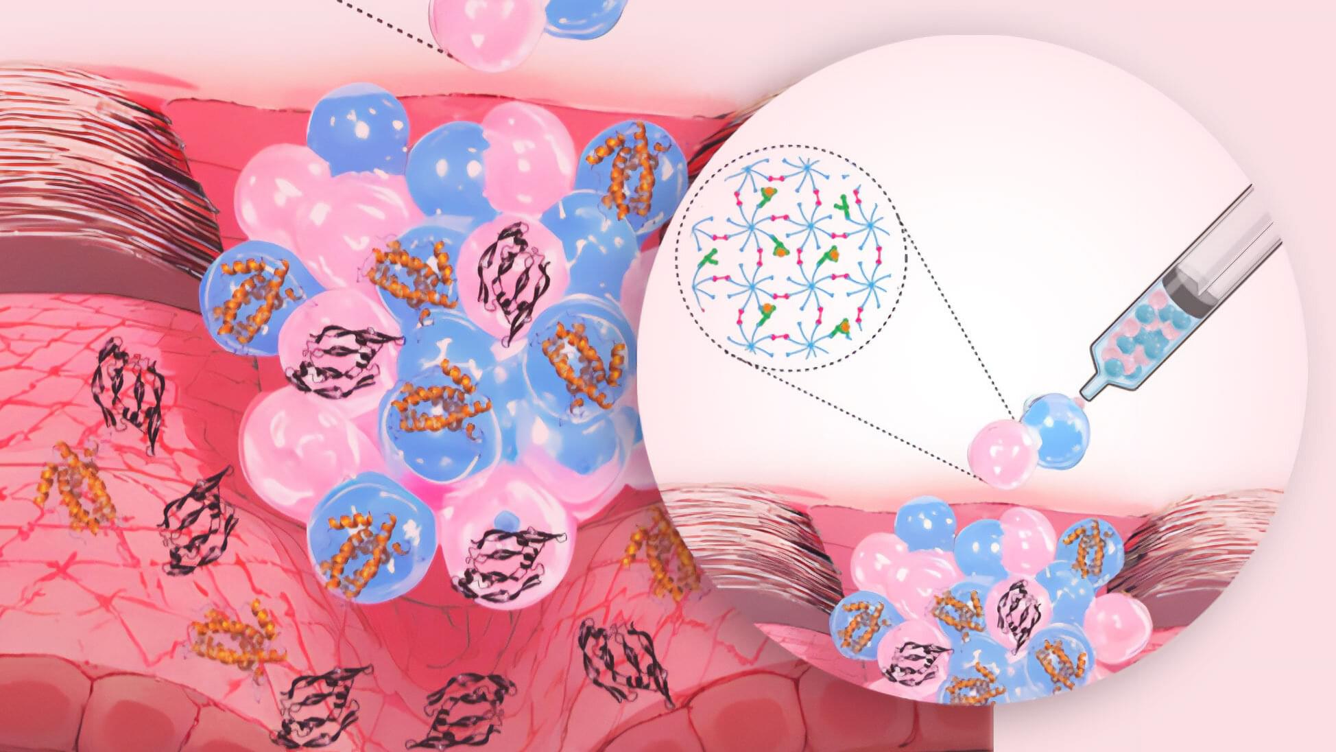
Chronic wounds are a major medical challenge, burdening health care systems with billions of dollars in costs every year. Pioneer Fellow Börte Emiroglu is developing a new product: a selective, sponge-like hydrogel that reduces inflammatory signals and actively promotes healing.
The work is published in the journal Advanced Healthcare Materials.
Emiroglu’s academic career has taken her from Turkey to Zurich, after a master’s degree, and straight into the interdisciplinary world of biomedical engineering at ETH Zurich. “Back then, I didn’t even know what a hydrogel was,” she recalls, thinking back to the early days of her doctoral research at the Macromolecular Engineering Laboratory under the supervision of Professor Mark Tibbitt.
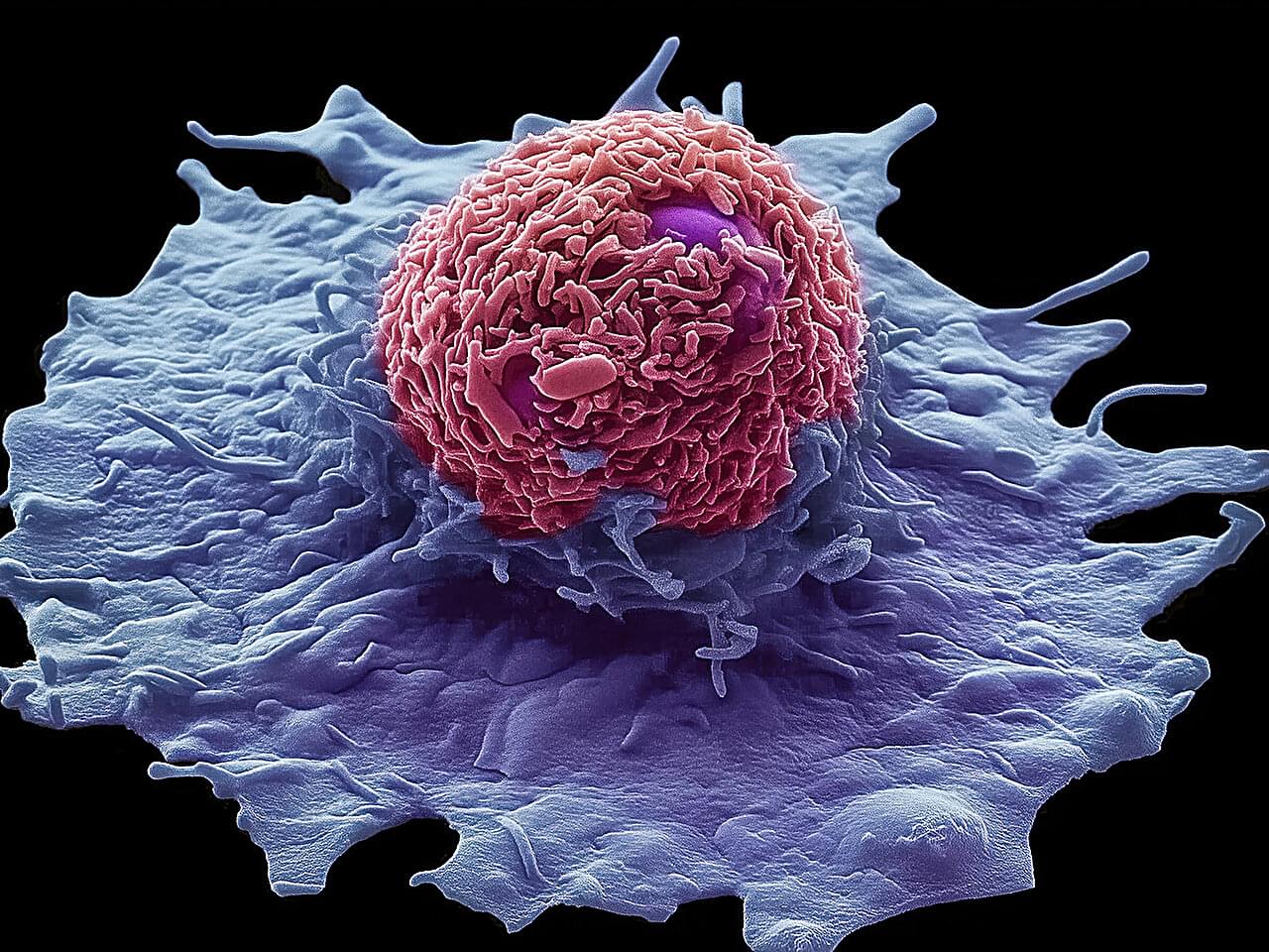
Lung macrophages play a pivotal role in diseases like idiopathic pulmonary fibrosis. Two types of macrophages—the white blood cells that defend the body by killing microbes, removing dead cells and stimulating immune responses—are found in the lung. They are tissue resident macrophages, which are present from birth, and monocyte-derived macrophages that enter the lungs for a short time in response to damage or infection.
Recently these monocyte-derived alveolar macrophages, or Mo-AMs, were identified as key drivers of lung fibrosis disease progression. However, the mechanisms of their pro-fibrotic behavior and survival in the lungs remained unclear, so clinicians continue to lack effective therapies.
In a study published in the journal Nature Communications, Gang Liu, M.D., Ph.D., Huachun Cui, Ph.D., and their University of Alabama at Birmingham colleagues show that TREM2, a cell surface receptor protein on Mo-AM cells, is a critical regulator of macrophage-mediated lung fibrosis. This makes it a promising therapeutic target for intervention, says Gang, a professor in the UAB Department of Medicine Division of Pulmonary, Allergy and Critical Care Medicine.
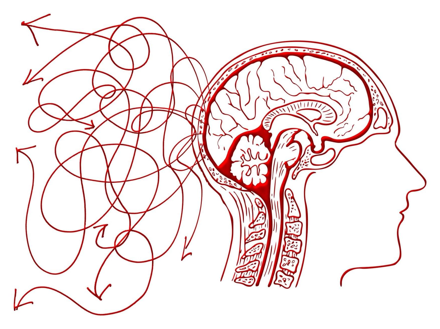
Researchers have long been interested in how humans and animals make decisions by focusing on trial-and-error behavior informed by recent information. However, the conventional frameworks for understanding these behaviors may overlook certain realities of decision-making because they assume we make the best decisions after taking into account our past experiences.
A newly released study by a team of scientists deploys AI in innovative ways to better understand this process. By using tiny artificial neural networks, the researchers’ work illuminates in detail what drives an individual’s actual choices—regardless of whether those choices are optimal or not.
The work appears in Nature.
The future of moon exploration may be rolling around a nondescript office on the CU Boulder campus. Here, a robot about as wide as a large pizza scoots forward on three wheels. It uses an arm with a claw at one end to pick up a plastic block from the floor, then set it back down.

For years, scientists have debated whether a giant thick ice shelf once covered the entire Arctic Ocean during the coldest ice ages. Now, a new study published in Science Advances challenges this idea as the research team found no evidence for the presence of a massive ~1km ice shelf. Instead, the Arctic Ocean appears to have been covered by seasonal sea ice—leaving open water and life-sustaining conditions even during the harshest periods of cold periods during the last 750,000 years.
The paper is titled “Seasonal sea ice characterized the glacial Arctic–Atlantic gateway over the past 750,000 years.”
This discovery gives insights crucial for our understanding of how the Arctic has responded to climate change in the past—and how it might behave in the future.
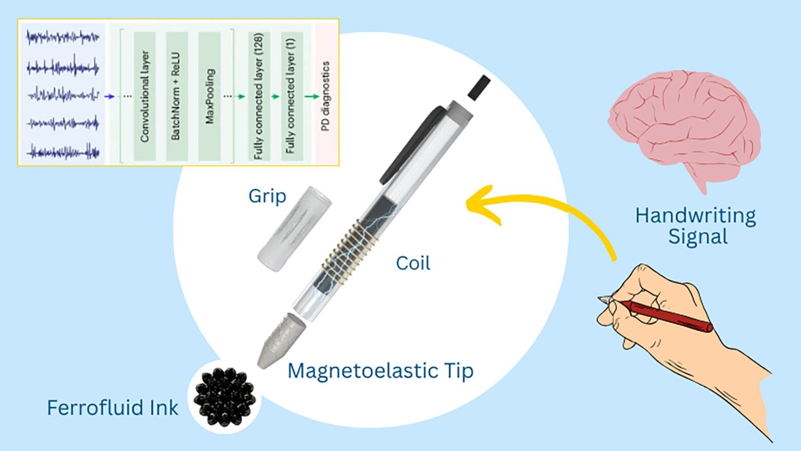
Every year, tens of thousands of people with signs of Parkinson’s disease go unnoticed until the incurable neurodegenerative condition has already progressed.
Motor symptoms, such as tremors or rigidity, often emerge only after significant neurological damage has occurred. By the time patients are diagnosed, more than half of their dopamine-producing neurons may already be lost. This kind of diagnostic delay can limit treatment options and slow progress on early-stage interventions.
While there are existing tests to detect biomarkers of Parkinson’s, including cell loss in the brain and inflammatory markers in blood, they typically require access to specialists and costly equipment at major medical centers, which may be out of reach for many.