Perovskites have been a hot research topic for the past 10 years, but we think we really have something here that can move us forward.
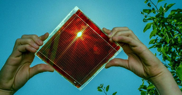

You might never have to plug the Reflect Eternal in for a recharge.
Another Tesla driver was caught sleeping behind the wheel on the highway.

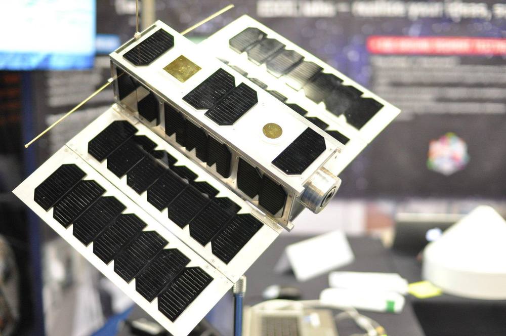
Calling all radio amateurs! We’re challenging anyone with amateur radio equipment to catch the first signals from #OPS –SAT, ESA’s brand new space software lab. On 17 December, OPS-SAT will be launched into space with ESA’s #Cheops exoplanet satellite.
Once launched, the satellite will deploy its solar panels and ultra-high frequency antenna, and then start to send signals back home. Could you be the first on Earth to catch them? ESA’s mission control team in Darmstadt are asking for your help to find the fledgling #CubeSat 👉 http://www.esa.int/Enabling_Support/Operations/Calling_radio…nd_OPS-SAT

Elon Musk has revived his idea to power the entire U.S. with one single, giant solar farm. In a recent tweet evidently directed at fellow mega-billionaire Bill Gates, Musk insinuated that his grand solar plan is actually quite simple (hat-tip to Inverse):
Decision-making algorithms transform how automated systems evaluate and synthesize novel compounds.
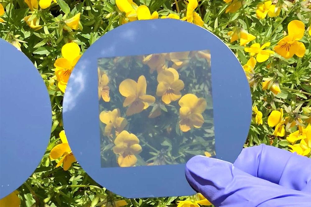
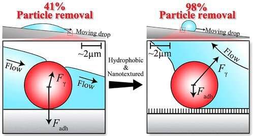
Taking a cue from the self-cleaning properties of the lotus leaf, researchers at Ben-Gurion University of the Negev have shed new light on microscopic forces and mechanisms that can be optimized to remove dust from solar panels to maintain efficiency and light absorption. The new technique removed 98 percent of dust particles.
In a new study published in Langmuir, the researchers confirmed that modifying the surface properties of solar panels may greatly reduce the amount of dust remaining on the surface, and significantly increase the potential of solar energy harvesting applications in the desert.
Dust adhesion on solar panels is a major challenge to energy harvesting through photovoltaic cells and solar thermal collectors. New solutions are necessary to maintain maximum collection efficiency in high dust density areas such as the Negev desert in Israel.

Every single member of the UN doubled-down today on a commitment to provide universal health coverage to their citizens. The fact that the US will be among them is perhaps evidence of how disconnected these declarations can be from actual domestic political agendas.
Yet the issue is important, and it shows just how out of line the US approach to health care coverage is compared to the rest of the world. Only about half the world’s population has access to the kind of affordable health care services that don’t require crippling out-of-pocket costs. Most of those people are in mid- and low-income countries. Or they are in the wealthiest country on Earth: the US.
Bringing universal health care to everyone is one of the “sustainable development goals,” the ambitious to-do list for UN member countries to complete by 2030. For the UN, universal health care means, “financial risk protection, access to quality essential health-care services and access to safe, effective, quality and affordable essential medicines and vaccines for all.”