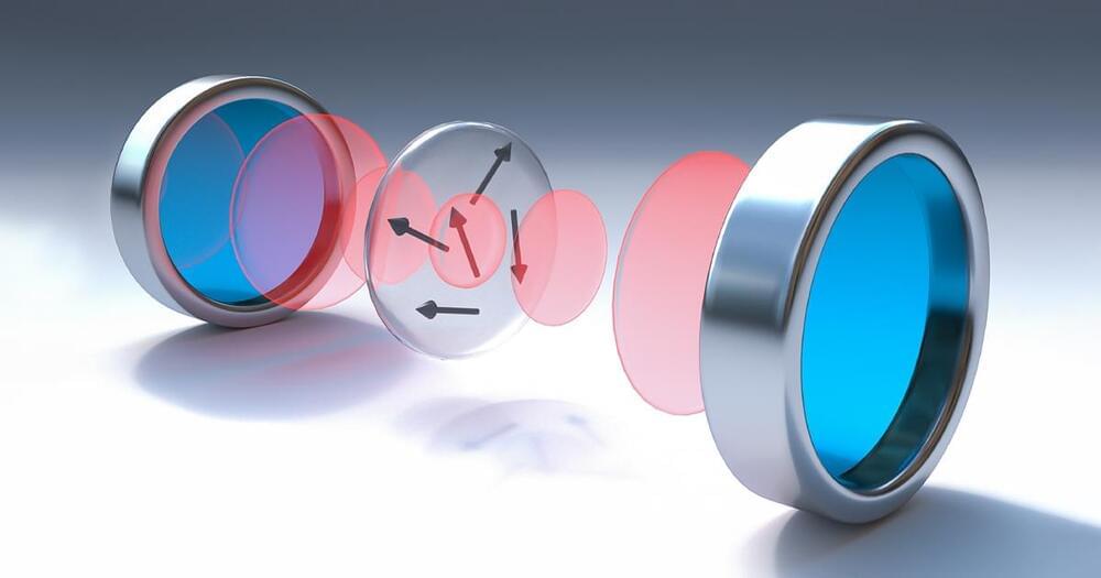
Lightspeed is the fastest velocity in the universe. Except when it isn’t. Anyone who’s seen a prism split white light into a rainbow has witnessed how material properties can influence the behavior of quantum objects: in this case, the speed at which light propagates.
Electrons also behave differently in materials than they do in free space, and understanding how is critical for scientists studying material properties and engineers looking to develop new technologies. “An electron’s wave nature is very particular. And if you want to design devices in the future that take advantage of this quantum mechanical nature, you need to know those wavefunctions really well,” explained co-author Joe Costello, a UC Santa Barbara graduate student in condensed matter physics.
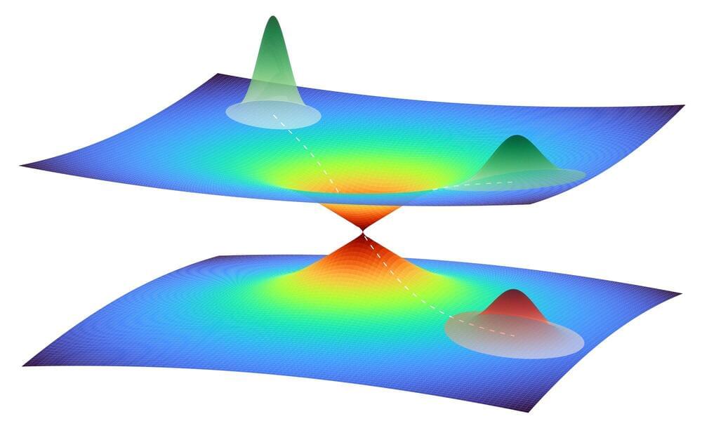
In a new paper, co-lead authors Costello, Seamus O’Hara and Qile Wu and their collaborators developed a method to calculate this wave nature, called a Bloch wavefunction, from physical measurements. “This is the first time that there’s been experimental reconstruction of a Bloch wavefunction,” said senior author Mark Sherwin, a professor of condensed matter physics at UC Santa Barbara. The team’s findings appear in the journal Nature, coming out more than 90 years after Felix Bloch first described the behavior of electrons in crystalline solids.